Adobe has deemed that the Flash content on web pages is too risky to be used by the general internet user. For virtually all modern browsers, support for Flash was eliminated on 1-1-2021. This means that those browsers will not display any of the interactive Flash demos/calculators/graphics on this (or any other) site.
The simplest (not the best) fix, for now, is to download the Ruffle extension for your browser. It will render the Flash files where they were previously blocked. In some browsers, you will have to click on the big 'play' button to make the Flash applets/graphics visible.
An alternative to Ruffle for viewing Flash content is to use an alternative browser like the older, portable version of Chrome (chromium), an older version of Safari for Windows or one of several other browsers. More information on Flash capable browsers can be found HERE. It's not quite as simple as Ruffle but anyone even moderately familiar with the Windows Control Panel and installation of software can use Flash as it was intended.
Navigation
This page is a bit longer than the other pages and may be somewhat difficult to navigate. Since it's designed as part of the Basic Car Audio Electronics site and you likely opened this page by clicking on item number 109 in the directory, that link should still be there. If you get in the middle of a long section and you want to quickly return to the top of the page, simply click the link in the directory for page 109. If there is no directory to the right, please click the arrow below and scroll down in the directory to page 109.
This page was created help you understand switching power supply basics. It applies only to push-pull switching power supplies powered from a 12v DC source (like those used in virtually all car audio amplifiers). It's not an in-depth tutorial and there is much more to learn but this should help introduce you to the basics. Most of the other sites and subject matter seem to be written for those who already know the material. This page is for those who know basic electronics but know absolutely nothing about switching power supplies. Hopefully, the information you find here will help you understand the subject matter well enough to understand the more advanced material you'll find on other sites. If you find that something is being discussed but some pre-requisite information seems to have been omitted, please email me. If you have questions, comments or suggestions regarding this material, feel free to email me.
If you're interested in building a switching power supply but are intimidated by the length of this page, don't be. Take it one section at a time. Give it time to sink in and a couple of days later, read another section.
Flash Based Graphics:
Most of the graphics on this site are Flash graphics. This means that they will not be visible on many of the internet capable cell phones and similar devices. If you're interested in this page, it's best viewed from a laptop or desktop computer.
~:
If you see the character '~', it means approximately. For example, ~15v means 'approximately 15v'.
B+:
B+ is the positive battery terminal connection on the amp, power supply or the positive 12v source (depending on the context).
4K7, 6K8...:
Abbreviations like 4K7 when referring to the values of components like resistors means 4.7K ohms (4700 ohms). You'll see this often when the value is printed on a component. Since the printing is often low quality on an uneven surface, it's easy to lose a tiny decimal point. The substitution of the K in place of the decimal point makes it unlikely that the value can be misread. The K means thousand. If you had a 2.2 ohm resistor, it would likely read 2R2. For a three million, three hundred thousand ohm resistor the marking would likely read 3M3.
g = AWG:
For this (and most of my tutorials), I substitute the letter 'g' for 'gauge' when stating the size of the wire. This is short for AWG (American Wire Gauge). 14g wire means 14 gauge wire.
xxx:
If you see a part number that has a lower case 'x' as part of the part number but the other letters of the part number are upper case, it means that there are several versions of the same basic part. For example the TLx94 could be a TL494 or a TL594 but, for the context, they are similar enough so that the TLx94 would cover both parts. The same goes for the L7815, L7805, L7809.... If the context was for the L78.. regulators in general, they would be referred to as the L78xx regulators.
'S' Suffix:
If you see a lower case 's' at the end of a part number (particularly one that has other letters in upper case), that's the pluralization of the part number and is not part of the part number. For example, If you're instructed to replace the 'IRF3205s' in the circuit, the part number is IRF3205, not IRF3205S.
Zooming in on Flash/Shockwave Files:
Many of the graphics files are Flash .swf files. You can determine which are Flash files by right-clicking while the mouse cursor is on the image. If it gives an option to zoom in, you can do so by simply selecting that option in the pop-up dialogue box. For files that have a relatively square format, if you've selected the option to open the image in a new window, you may want to use the F11 button to go to full screen. You can zoom in when in full screen mode if you want to see the file at a higher resolution. The vector graphics files (most of the schematic diagram files and interactive demos) can be enlarged significantly with no loss of quality. The Flash files that contain bitmap type images have a finite resolution and zooming in more than one time generally won't provide any better detail. While zoomed-in, you can use the left mouse button to scroll/navigate.
Note:
Most browsers toggle from full screen to normal viewing with F11 but Firefox won't. To get back to normal viewing, you must go to the top-right of the display and click the restore button (between the minimize button and the X).
Dead Links:
For those reading this online, you'll find links that are dead. This was primarily written as part of the Car Audio Amplifier Repair Tutorial. Some of the links here will point to links in the tutorial so they will not work online. It's too time consuming to have more than one version so I've left the links. If you're reading this as part of the tutorial and find a dead link, please email me.
Links that Open in Pop-Up Windows:
Some of the links and images open in pop-up windows. Many people click on the main window to make the pop-up fall behind the main window. If you click on another link that is supposed to open on top of the main window, it may not and it may appear that the link isn't working. The link will open in the previous pop-up window that's now behind the main window but you may not notice it unless you see the moving icon on the browser tab as the content loads. To prevent this from happening, close each pop-up by clicking the 'X' at the top of the pop-up window.
Power Supply vs Regulator:
The terms switching power supply and switching regulator can, many times, be used interchangeably. On this page, I'll try to differentiate between the two. A switching power supply will refer to a circuit that boosts the voltage. The sample switching power supply on this page boosts the voltage from 12v to �36 volts (or more, depending on the transformer). A switching regulator refers to a circuit that takes a voltage greater than the regulated output voltage then reduces and stabilizes the voltage. Both switching and linear regulators will perform this function. Technically, the sample power supply could be considered a switching regulator if it uses regulation to maintain a specific output voltage but since that voltage is always going to be greater than the 12v input voltage (from the vehicle's charging system), it will be referred to as a regulated power supply instead of a switching regulator.
Power Supply to be Used as an Example in this Tutorial
The power supply below is the one that we'll use as a basis for this tutorial. It was designed to be used with audio power amplifiers but can be used for virtually anything that needs DC voltage greater than what's available from the automotive charging system. If you want to build a switching power supply to power an audio amplifier that you originally built to operate off of mains power but now want to use it for car audio, this type of supply will work very well.
Many tutorials start by showing the individual parts/circuits but you have to wait until late in the tutorial to see how the individual circuits work together. This first section is to help those who prefer to know where they're going before they begin their journey.
Basic Features of this Power Supply
Output Power:
This power supply can support an 800 watt audio power amplifier. To operate at full power for extended periods, the power supply will need a fan to force air over the internal components and heatsink to keep it cool. The heatsink (the one used for testing) generally remains relatively cool but the internal components will benefit by having air flowing over/around them if the supply is run to full rated output. With an audio amplifier bridged into 4 ohms, regularly driven into clipping (music) and with the supply's rail voltage initially set to ~94v across the rails (�47v), a 50mm x 10mm fan easily kept the heatsink and internal components cool.
To clarify for those who may want to build this supply or a similar supply, this power supply is designed to supply power to an audio amplifier. When it's stated that it can provide 800 watts, that's not a continuous 800 watts DC output (100% duty cycle). It's designed to provide the power to an audio amplifier that intermittently draws the power required to produce 800 watts. To provide a continuous 800 watts of straight DC, the power supply would have to have approximately twice the components as this one.
As a test, the prototype supply was connected across a 4 ohm resistor. The 12v power supply (actually 13.18v during testing) couldn't supply enough current to drive more than 54.7v (1:3.75 transformer with regulation) into the load. It was driven into the 4 ohm load for 27 minutes, until my 12v power supply shut down (too lazy to unbury a larger 12v supply). There was no damage to this supply but the temperature of several of the components indicated that it was being driven about as hard as it could be without going into thermal shutdown. This is a MUCH harder load than if it were driving an amplifier to clipping.
Test with 1:3 transformer... 12.7v DC driving a 4 ohm load, the power supply produced 64.8v across the load.
Thermistor Protection:
This power supply has a fan drive circuit that's controlled by the temperature of a dedicated thermistor (Power Supply Troubleshooting, #27). The thermistor can be placed on the heatsink or the components that operate at the highest temperatures (whichever you decide to let control the fan speed - I generally place it on the primary filter capacitors). The fan speed control is crude but variable. For this supply, you don't need a fan moving large amounts of air. A minimal amount of air flow will make a huge difference in the temperature of the components.
There is a second dedicated thermistor that's used for thermal protection of the supply. The supply is designed to shut down at ~80C (~176�F). The thermal protection employs 'hysteresis' which requires that the supply cool down to ~68C (prototype temperature readings) before it will power on again. The shutdown temperature can be changed by changing the value of the resistor in series with the thermistor. A lower value will make the shutdown temperature increase.
Regulation of Main Rails:
You can operate this power supply with or without regulation. When operated with regulation, both the positive and negative rails are monitored. The regulator has a potentiometer to allow precise voltage adjustment. If you want to have a regulated power supply, I recommend 'over-winding' the power transformer to no more than 20% over what's needed to produce the desired output voltage. This may not be a tightly regulated supply if excessive current is drawn by the amplifier but it's typically good enough and is more efficient than a tightly regulated supply (which requires more over-winding).
Pre-Regulators:
The pre-regulators in this power supply allow the �15v IC regulators (L7815 and L7915) to be used with rail voltage greater than the regulators' maximum supply voltage. The 7815/7915 regulators aren't designed to withstand more than 35v of supply voltage. If you have the main supply set up to produce more than �35v, they need something to limit the voltage feeding them. That's one reason for the pre-regulators.
The pre-regulator outputs can be used to supply power to 'chip-amps'. The maximum input voltage for many of the chip-amps is �25-30v DC. Many people want to have a large bass amp and smaller 'chip-amps' for the rear/door/dash speakers. The bass amp can be operated from the main power supply. The chip-amps will operate off of the pre-regulators. The supply was designed to allow the user to power a sub amp from the main rails and chip amps from the pre-regulators. If you're only going to use the supply to power the chip-amps, use the main rails for the chip-amps instead of the pre-regulators. This will result in much lower operating temperatures. The pre-regulators (and the IC regulators) are linear voltage regulators and will produce quite a bit of heat. In some instances, you may need to use a high output fan to provide enough cooling. If you use the main rails for your amp (set to the proper voltage for the chip-amps), the power supply will operate at a much lower temperature.
The pre-regulator transistors have no protection circuits and could be damaged if their output is shorted to ground or one of the other power supply outputs. I strongly recommend that you use inline fuses in the wires that you use to connect to the pre-reg output. A 7.5 amp fast-blow fuse should be sufficient to protect the transistors.
�15v Regulators:
The IC voltage regulators provide clean power for the audio op-amps that will be used for the preamp section of the power amplifier(s). The L7815 and L7915 (Audio Troubleshooting, only available on the amplifier repair DVD, item #26) provide an extremely stable output voltage and employ over-current/short-circuit protection as well as thermal protection. This makes them very reliable. The 15v regulators are generally the best choice but if you want to use regulators with a different output voltage, that's up to you.
If the rail voltage for the main power supply is set to less than �35v, the pre-regulators don't need to be used to reduce the supply voltage for the IC voltage regulators. If they're not needed for any other purpose (chip amps, etc...), the pre-regulator power transistors can be omitted and bypassed (leg 2 shorted to leg 3 with a jumper wire). Since the pre-regulators won't be used, there's no need to install any of the resistors, capacitors or diodes associated with them.
Bypass Capacitors:
All supplies are bypassed with film capacitors. Power supplies (especially switching power supplies, like this one) need significant filtering to remove the ripple from the output. Large aluminum electrolytic capacitors (round cylindrical devices on the board) are best suited to provide large amounts of capacitance. This removes most of the noise but aluminum type electrolytics may not filter the highest frequency noise as well as film capacitors. To more effectively remove that noise, smaller value film capacitors are used. They are connected in parallel with the electrolytics and together, they do a good job of bypassing all of the noise to ground.
Notes:
There is some disagreement as to whether the 0.1uF bypass capacitors are necessary, beneficial or detrimental to the proper operation of a power supply. Since there are a lot of variables that could make them any of those, you can decide to use them or leave them out. Since I haven't experienced any problems using them, I'd suggest that you initially install them and only omit them if there is a problem. This only applies to the bypass capacitors located near the electrolytic capacitors that they're bypassing. It does not apply to other 0.1uF capacitors. Those are required for the proper operation of the power supply.
Previously, the term 'noise' was used. Since switching power supplies typically operate at 25,000Hz or higher, the 'noise' is well above audio frequencies and rarely becomes audible but can sometimes work it's way into the audio chain. In general, the 'noise' is high frequency noise at some multiple of the operating frequency. In some instances, this noise can be transmitted outside the power supply and can cause interference with radio transmissions. If you've ever had a class D amp that interfered with your am/fm radio reception, that was RFI (Radio Frequency Interference) and was caused by the noise generated by the amplifier's switching circuitry.
Output Filter:
The main output uses an LC filter. To reduce stress on the filter capacitors (particularly when the power supply is used in regulated mode), an LC (inductor/capacitor) filter is used instead of only using a filter capacitor. This also provides a slightly cleaner output but the main purpose of the inductor is to take stress off of the filter capacitors.
Secondary Ground Offset Protection:
There is an opto-coupler that monitors the DC voltage on the secondary ground. This will shut the supply down if the output of the supply shorts to chassis ground. It will also protect both the supply and the amplifier if a live speaker wire shorts to chassis ground. The opto-coupler shuts the supply down when the secondary ground is 2v above or 2v below the chassis ground voltage (0v DC).
Internal Fuses:
The internal fuses are in series with the main rails of the supply and help protect the supply from excessive current draw. These are typically going to be 15 amp fuses but the required value may be different depending on the output voltage selected. If the supply is used for an amp that needs only �20v, the fuses could be increased to 20 amps. If the supply was going to be used at �60v, the fuses would have to be reduced to 10 amps.
External Fuses:
There was insufficient space on the circuit board to provide an on-board fuse for the B+ input. The power supply MUST be fused externally with a 50 amp fuse. I'd recommend either a MAXI-fuse or an AGU fuse (only Bussmann or Littelfuse brands, for proper protection). Failure to use a fuse can lead to catastrophic failure of the power supply. Sometimes, the damage is so severe that the supply will be irreparable.
Important:
If you blow the main power fuse feeding this power supply, it's strongly recommended that you not simply insert a new fuse of the same size. When in good working order, the power supply draws only about 1 amp at idle. After the fuse blows, remove the load from the power supply (or at the very least set the volume control on the signal source to the minimum position) and install a 10-20 amp fuse in the main fuse holder (the one where the 50 amp fuse was installed). If the fuse blows, you will have to disconnect ALL loads from the power supply and try it again. If the 10-20 amp fuse blows with no loads connected to the power supply, the supply has likely failed and will need to be repaired. Do NOT (repeat, do NOT) install a fuse larger than 50 amps and do NOT bypass the fuse. Wrapping aluminum foil around the fuse WILL cause catastrophic failure of the supply and will almost certainly make the power supply irreparable.
Thermal Protection for the Audio Amplifier:
An input is provided for thermal protection of the amplifier that will be powered by the supply. The amplifier needs to have a normally-open thermostat. When the thermostat closes (at excessive temperatures), the supply will shut down. The thermostat must be completely isolated from all power supplies and ground (dry contacts).
LED Drive Indicators:
This supply is designed to be easy to troubleshoot without having an oscilloscope. All outputs on the terminal block (�rail and �15v) have LEDs that show they're producing output. There is an LED to show that the amp is receiving remote turn-on voltage. There are two other LEDs on the power supply drive circuit that show that the drive circuit is working. These only illuminate when there's oscillation (drive signal for the power supply FETs). They will not illuminate when there is only DC. These can be omitted if not needed. They were mainly included for those who didn't have a way to determine if there was oscillation/output from the drive circuit.
Auxiliary Power Supply:
There is an auxiliary power supply that can be used in several ways. Normally, this will be used to produce 'greater_than_rail' voltage for the driver circuits in the audio amplifier. It can be used to produce both positive and negative voltage, only positive voltage or only negative voltage. It can be used with isolated windings or with windings added to the secondary windings. Additional through-holes are provided to allow connecting the auxiliary windings to the secondary windings or to the secondary ground. This supply is only capable of providing approximately 1 amp of current. But that's sufficient for the driver stage of an audio amplifier.
Note:
The term 'winding' refers to a group of turns/wraps around the core of the transformer. Examples are primary windings, secondary windings and auxiliary windings. The term 'turns' refers to the individual loops of wires. The primary windings (those driven by the power supply FETs) will typically be two groups of 4 turns each (commonly referred to as a 4+4 configuration). For many transformers, the wire used for the windings will be stranded. It could be 2, 3, even 30 strands of wire that make up the wire used for each turn. These paralleled strands act as one wire and don't count as individual turns. For this supply, three parallel-connected strands of 14g wire make up the wire that's used for the primary windings.
Aux Supply Option 1:
Using 4 turns for each of the two auxiliary windings. One winding will have it's ends in points A and C. The other will have it's ends in points B and D. This will give an output of rail voltage plus ~B+ voltage. The voltage will be equal to the rail voltage plus (the B+ supply voltage * number of turns/4).
Aux Supply Option 2:
Using two windings and having one end of the aux windings in the secondary center tap and the other end in C and D, the output will be plus/minus B+ voltage * number of turns/4.
Aux Supply Option 3:
Having only a single winding and using only C and D, the output voltage will be B+ * the number of windings/4.
Heatsink Ground:
A ground is provided for the heatsink. This will help shunt any noise from the sink to chassis ground. It is designed not to burn when the heatsink is shorted to 12v (which sometimes happens if the power connections are made while the B+ wire has voltage on it).
Gate Resistors:
It has separate drive resistors for turn-on and turn off resistors (for the gates of the power supply FETs). This allows you to fine-tune the value of the resistors to get the cleanest square wave on the power supply primary windings.
Snubbers:
Snubbers (RC networks) on the primary windings help damp any remaining ringing on the primary waveform.
Secondary Ground Isolation:
The power supply has an isolated secondary which simplifies the design of the power amplifier. Virtually all car audio power amplifiers need isolation from chassis ground for their RCA shield ground. The simplest way to do this is to have an isolated secondary ground. It can also be done by using a noise-cancelling or a balanced input circuit. These are not difficult to design but add to the complexity of an amplifier.
Switching vs. Linear:
On the Amplifier Classes page (you should go read that (short) page now if you haven't done so), I stated that you could use the simple analogy of someone holding a weight at an average height to simulate the two types of systems (switching/linear). If you told two people to hold a weight at an average height of 5 feet above the ground, one might hold it straight out from their body at a constant height. The other person (a more efficient person) might hold the weight with their arm straight down half of the time and straight up the other half of the time. This would average approximately 5 feet above the ground. The person holding the weight straight out constantly would get fatigued/tired much more quickly than the person holding the weight with their arm straight up or straight down. The person holding the weight straight out would be analogous to a 'linear' power supply (or maybe more accurately, a linear voltage regulator). The person holding the weight up or down would be analogous to a 'switching' power supply. For this part of the tutorial (where we'll go into more specifics), we need to make the analogy a bit more complex. The reasons for the added complexity will become apparent as the tutorial progresses.
You can think of the fatigue as loss or stress on the system. In the world of electronics, this loss is typically in the form of heat and it reduces the efficiency of the system as a whole.
'System' Requirements:
For this example/analogy, we need a system that can provide a constant, steady stream of water. Let's assume that it's a system that is used to water a delicate plant. The only source of water is a fire hose. Obviously, a fire hose can easily deliver enough force (voltage) and flow of water (current) to destroy the delicate plant.
Linear system:
In a 'linear' system you would have a constant, steady stream of water flowing directly from the nozzle on the fire hose. The flow would be regulated by the person holding the valve on the hose at precisely the correct position to deliver the desired flow. After a while, that person's hand would become fatigued. This would be a very simple, inexpensive system but it's inefficient.
Switching System:
In a 'switching' system you would have pulses of water delivered at a rate much greater than you could use if the stream from the source was delivered directly. Since the pulsing the water on and off wouldn't produce a constant, steady, gentle stream of water, you'd need some sort of reservoir. Here, let's imagine it's a bucket partially filled with a sponge-like material and a hole in the bottom of the bucket. For the flow out of the bucket to be at the proper rate, the bucket would need to be approximately half full. Here, you'd either hold the valve on the fire hose either fully open or release it to stop the flow. The pulses have to be timed just right or the bucket would be filled too full or would run dry. This would produce much less fatigue than the 'linear' system. It's more efficient but it's more complex.
As you can imagine, the pulses of water into the bucket would produce lots of splashing. This would be similar to high frequency 'noise' generated by the switching system. You'd have to make an extra effort (more components) to prevent the area around the bucket from getting splashed. Again, this adds to the complexity and cost of the switching system.
Linear Power Supply:
Above, we saw water analogies of the two types of power supplies. Below is the most basic linear power supply (except possibly for a battery). In this circuit, the output of a power transformer is rectified (which converts it to DC). The rectified DC (which has a lot of ripple) is filtered by a capacitor. Many times, the load is connected to filter capacitors directly with no other components needed. For more on Rectification and Filtering, read THIS page.
For regulated linear power supplies, a voltage reference of some sort (often a Zener diode) is used to deliver a constant voltage from a not-so-constant power source. For instances where the current draw requirements will be significant, a transistor is used to boost the current (above what the Zener reference circuit could deliver). In car amps, the rail voltage (the power supply for the power amplifier circuitry) often has a lot of variation. This variation/ripple is caused by varying current demand by the power amplifier driving the speakers and also from varying supply voltage from the vehicle. The ripple can cause noise or instability issues in some circuits (that's why the regulator is needed). The output of the regulator transistor is often directly connected to the load being powered by the regulated power supply. One example of this is the regulator that uses a Zener shunt regulator to feed the base of a current-boosting transistor. A linear power supply is simple, requires few parts and produces a clean output voltage with very little filtering needed (often only a single, small capacitor). The problem with linear power supplies and regulators is that they're not efficient which means they waste a lot of energy and can produce significant heat.
The following shows two typical power supply voltage regulators (one for positive regulated voltage and one for negative regulated voltage). As you can see, they require only a few parts. These are used in all sorts of equipment. For audio amplifiers, they're typically used to supply power to the preamp components (which can't withstand the full rail voltage in the amplifier) or other circuits that require a relatively noise free voltage source. In a real circuit, the emitter of the output transistor would be connected to a capacitor. The other terminal of the capacitor would be connected to ground.
There are several types of switching regulators. The switching regulator most like the linear regulator above is the 'buck' regulator. The buck regulator is used to produce an output voltage less than the input voltage. The 'boost' regulator is used when the output voltage needs to be greater than the input voltage. There's also a buck/boost regulator that can produce voltage greater than or less than the input voltage. For switching regulators, in general, the output transistor is switched on and off at high frequency (25,000Hz or more, typically). The output transistor can't drive the load directly (in most cases) due to the high frequency 'noise' that is generated by the switching of the transistor. To filter the noise, the output transistor drives an inductor. The output of the inductor goes to a capacitor that has it's other terminal connected to ground. The capacitor bypasses/shunts virtually all of the noise/ripple to ground so that none is passed to the load being driven/powered by the supply/regulator. For a switching regulator with this simple filtering, the load is connected to the point where the inductor connects to the capacitor. The inductor and capacitor act as the 'bucket and sponge' described previously. They help convert the pulses to constant, smooth, steady voltage. This produce the same type of output as a linear supply but the drive circuit required to switch the transistor on and off at the proper rate and the (relatively expensive) inductor make this type of system much more complex. It is, however, much more efficient and sometimes efficiency is more important than the complexity of the circuit.
Switching power supplies are very common. The computer you're using right now has a switching power supply with several output voltages (+12, -12, +5, -5, and +3.3v, at least). These outputs are taken by the mother board and, in some instances, regulated down even further. For example, the 12v output is often regulated down to well below 1.5v to supply power to the microprocessor. The photo below shows the switching regulator components on a computer motherboard. The green arrows point to; A: transistors, B: capacitors, C: inductors.
If a modern computer used a linear power supply to convert 12v down to ~1.3v (approximately what's presently used by many CPUs), it would produce a tremendous amount of heat. Many microprocessors can draw more than 100 amps of current. CPUs (microprocessors) are designed to operate at relatively low voltage so the processor can operate more efficiently and therefore produce less heat.
Now, back to the 12v to 1.3v regulator...
If you remember Ohms Law (actually Joule's Law), the power dissipation is the voltage across a device multiplied by the current passing through that device (P=E*I P: power; E: voltage; I: current). If the motherboard used a linear regulator, the power dissipation by the regulator transistor(s) would be the voltage drop from 12v (supply voltage) to 1.3v (output voltage) times the current (100 amps). That's over 1000 watts. The regulator would produce nearly as much heat as a blow dryer (type used to dry your hair) set on the highest setting. This would be inefficient and would make it VERY difficult to keep the computer case cool. The switching regulators used in computers can provide regulation while dissipating only a tiny fraction of the power of a linear regulator. If you're interested in learning more about linear voltage regulators, THIS page has an example of a variable regulator that can be used for all sorts of projects.
Need Help?
If there was anything in the previous section that was not clearly explained (either in the text or on the linked pages) or if you have questions about something covered above, email me.
Overall View:
This is the same basic supply you saw at the top of this page. Without the heatsink, you can see all of the power semiconductors along the edges of the board. During normal operation (when the supply is producing significant output current), these power semiconductors must be clamped tightly to the heatsink. Without the heatsink to soak up the heat that they produce/dissipate, they would fail within seconds. Using this supply, you will be shown the various circuits. Some of the basic design calculations will be included later in this part of the tutorial. it's possible that the circuit boards and heatsinks will be made available at a later date but that depends on the demand for them.
Note:
On this page, you'll see several different versions of the sample power supply. All are essentially the same and perform the same basic functions.
Schematic Diagram:
The following is a schematic diagram for this power supply. As this tutorial progresses, each of the sub-circuits that make up the power supply (as a whole) will be covered in more detail.
Click HERE to open this in a new window. Right click to Zoom-in. Left click to scroll.
Power Transformer:
In the next photo, the green arrow points to the transformer as a whole. The red arrow points to the toroidal (round) core. Other core shapes are common but only the toroidal core will be covered on this page.
Toroidal Core:
It's not obvious but the material that makes up the core is very important and has to be chosen based on the intended use. Many people make the mistake of trying to build power transformers with cores salvaged from computer (or other) switching power supplies. In computer power supplies, the toroids are typically used for output filter inductors and are made of a very different material than the cores used for power transformers. The two types of cores are typically not interchangeable (even though they may appear to be identical). Using the wrong type of core causes a lot of beginners to give up on trying to build a supply when they can't get it to work properly. From the email I've received, this is the most common problem when people have trouble with overheating FETs or excessive current draw with no load on the supply. For power transformers, you'll typically use 'ferrite' cores. For inductors, you'll typically use 'powder' cores. Powder cores include molypermalloy cores, sendust cores, Kool mu cores and high flux cores. Ferrite cores used for power transformers typically have a much higher 'permeability' (to be covered a bit later), compared to the cores used for inductors. One instance where you may use ferrite cores for inductors is when you have a common-mode inductor/choke but for most other inductors, you'll use powder cores.
The toroidal core is only one of many that can be used for transformers or inductors. EI and ETD cores are more common in equipment manufactured in large quantities or where the number of turns is significantly higher (as in power transformers operated off of the mains in your home). For more information on the various core shapes, click HERE.
For power transformers, my core material of choice is 'P' material. 'F' material also works well. The core in the sample supply is a ZP44916-TC. I think it's been superceded by the ZP44920-TC. 'Z' is the coating. 'P' is the material from which the core is made. The numbers roughly give the dimension (very roughly). 'TC' indicates that it's a toroidal core. For inductors, I prefer to use molypermalloy cores but they're significantly more expensive than cores made of other material.
Capacitors:
In the power supply we're using as an example, there are several relatively large cylindrical capacitors. These are 'electrolytic' capacitors and are used for filtering. Electrolytic capacitors are almost always used where significant capacitance is required. There are also several smaller orange/brown capacitors. These are 'film' capacitors. Most of the time, the 'film' used to make the capacitor is Mylar (polyester) so these are often referred to as Mylar capacitors. Mylar is Dupont's trade name for the polyester material.
Rectifiers:
Rectifiers are used to convert the AC output voltage from the power transformer to positive and negative DC voltage. In some amplifiers and power supplies, you'll find dual rectifiers. They are generally 3-legged devices. There is one positive rectifier (positive output on center leg) and one negative rectifier (negative output on center leg). Here, there are 4 individual rectifiers.
LC Filter:
In this photo, the green arrow points to an inductor. This inductor and the filter capacitors work together (remember the bucket and sponge from earlier on this page) to filter the pulses from the rectifiers. The red arrows indicate the filter capacitors that are working with the inductor to perform the filtering duties. The capacitors indicated by the yellow arrows are essentially in parallel with the 'red' capacitors but don't perform any real filtering due to their size (which is swamped out by the large electrolytic filter capacitors). They are simply there to keep the supply stable when/if the rail fuses (blue, 15 amp) open/blow. The 100uF capacitors are omitted in the next version of the board (rev. 3) since the output filter capacitors are connected to the input side of the fuse instead of the output side of the fuse. For the inductor in this supply, there are two stacked cores. This essentially doubles the inductance per number of turns. The cores used here are the CM270125. They were purchased from CWS Bytemark.
Previously, it was stated that this supply could be operated with or without regulation. This 'regulation' is the regulation of the voltage on the main supply rails (the ones that will drive the power amplifier's output transistors). For unregulated power supplies, the deadtime between the pulses of the power supply is so short that a filter inductor isn't needed. Since this supply was designed to allow regulated operation, the inductor is used in the output filter. When using regulation, the deadtime between pulses is significant. If there is excessive current draw and significant deadtime, the filter capacitors could be stressed which could cause them to overheat and fail. The inductor stores and releases energy to help reduce the stress on the capacitors.
Control IC:
Virtually all switching power supplies have a dedicated control IC (yellow arrow). The ICs typically used in car amplifiers are the TL494, TL594 and the SG3525. The TL494 and the TL594 are essentially identical and will be referred to as the TLx94 or TL594 IC. These ICs have various inputs that determine the duty cycle of the output pulses. Some inputs are used to shut down the supply if there is a problem. Other inputs allow the IC to regulate the output voltage of the power supply. The ICs like the SG3525 and SG3526 can drive the power supply FETs directly but in high power supplies, they drive an emitter follower pair (two emitter follower pairs indicated by the green arrows). ICs like the TL494 and TL594 are rarely every used to drive the power supply FETs directly and will almost always have a PNP driver transistor (half of an emitter follower pair) to drive the power supply FETs.
Above, it was stated that most power supplies had a dedicated control IC. In older (or simpler) switching power supplies there was no control IC. These power supplies were self oscillating. They typically had extra windings on the power transformer that were used to drive the driver transistors which in-turn drove the power transistors (which drove the power transformer). These were used in the early Rockford Punch 45s, 75s and 150s. They were also used in the early Linear Power amplifiers.
It was also stated above that the TLx94 and the SG352x ICs were the most commonly used driver ICs. There are a few amplifiers (specifically, Stetsom amplifiers) that use a PIC microcontroller to drive the power supply and to process the protection circuit logic. These won't be covered here but if you're interested in power supply design, you should be aware that this type of drive circuit exists.
Resistors on Emitter Follower Pair:
There are several resistors connected to the emitter follower pairs used to drive the power supply FETs. There are two 330 ohm 1/4 watt resistors. These are used as pulldown resistors. The output of the TL594 has very little ability to pull the voltage down on its output pins (pins 9 and 10 for this supply). The 330 ohm resistors pull the voltage down quickly to ensure that the output drive voltage is as low as possible before the other output switches on. If both outputs are on at the same time, the power supply FETs would fail. If the design of the circuit is marginal, the FETs may be on at the same time for a tiny fraction of a second. This won't lead to instantaneous destruction of the FETs but it will make them operate at relatively high temperatures (even when the supply has no external load). Having both banks of FETs on at the same time is called 'shoot-through'. It's not generally a problem with power supply FETs but if you ever design a class D amp, you'll have to try to minimize deadtime and will likely have shoot-through as you optimize the switching of the output FETs.
The 330 ohm resistors are only part of the drive circuit. In most power supplies, there are gate resistors. These are the resistors connected to the gates of the power supply FETs. This supply has the normal gate resistors but to allow tweaking, individual resistors are connected to the output of each of the transistors of the emitter follower pairs. This allows you to change a single resistor for each emitter follower pair to tweak the switching of the power supply FETs. This tweaking may be necessary if you use any FET other than the IRF3205s used in the prototype. Tweaking the values allows you to minimize turn-on and turn-off transients on the drains of the FETs. This can be important if you're using the supply for an audio amplifier and are trying to measure the THD+noise of the amp. The switching transients will rarely cause audible noise but it can be a problem when measuring noise with sensitive test equipment.
When using the supply with output regulation and you're experimenting with various values for the drive circuit resistors, it's important that you either defeat the regulation or reduce the input voltage far enough to force the supply to go to full duty cycle. This is important because you may have values that allow the supply to operate properly at low duty cycles but when at full duty cycle, the FETs may not be switched off fully allowing shoot-through. Without forcing the supply to full duty cycle under no-load conditions, you may never know there's a problem. The easiest way to check this is to note the idle current when the duty cycle is low and then again when at full duty cycle. If the current is higher at full duty cycle, there is a problem. This assumes that the output voltage of the supply hasn't exceeded the rated working voltage of the filter capacitors. When doing this test, lowering the input voltage to force the duty cycle higher is the best method of testing.
If you don't need to tweak the values for turn on/off of the FETs, you can replace the resistors on the emitters of the follower pairs with wire jumpers and use the appropriate resistor for the gate resistors. For the IRF3205s, a 47 ohm gate resistor works well.
Minimum Component Set:
Although the IC has many more components connected to it, only a few are required for the IC to produce output pulses. They are shown below. Of course, the IC needs a power source. The B+ power supply connection for the IC is pin 12. The ground terminal for the IC is pin 7. When there's more than ~6.5v across pins 12 and 7, the IC will power up and produce 5v on pin 14. To make the IC oscillate at the correct frequency, you have to have the timing components. These are the resistor and capacitor on pins 5 and 6 of the IC. One terminal of each connects to the IC. The other end of the timing resistor and capacitor connects to ground. With only those components connected, the IC's oscillator will produce a sawtooth waveform on pin 5. The frequency of the waveform can be calculated by the formula f = 1.1/RC. The frequency given by the formula is twice that of the output frequency of the waveforms seen on pins 9 and 10 (typically used as the output pins). I typically use 0.001uF for the timing capacitor and a 20k ohm resistor for the timing resistor. This produces an output frequency of approximately 30kHz. If you want to ensure that the oscillator frequency doesn't drift significantly with changes in temperature, you need to use a capacitor with a 0 temperature coefficient. This means that the value of the capacitor won't be affected by a change in temperature. For there to be drive/output pulses on pins 9 and 10, you need to have supply voltage on pins 8 and 11. Many times, these are connected directly to pin 12. The error amp input pins 1, 2, 15 and 16 (more on those later) need to be connected as shown to ensure proper operation when they're not being used.
Power Supply FETs:
The power supply FETs (Field Effect Transistors) drive the 'primary' windings of the power supply transformer. The IRFZ44 and IRF3205 are (at this time) popular transistors for switching power supplies. This supply was designed to use IRF3205s but can be used with virtually any FET that can withstand the current demands created by the current draw from the output of the power supply. These power supply FETs are driven by the emitter follower pairs shown in the previous photo that showed the control IC.
Need Help?
If there was anything in the previous section that was not clearly explained (either in the text or on the linked pages) or if you have questions about something covered above, email me.
Topology:
There are many types of switching power supplies. The one we're working with here is a 'push-pull' power supply. This is what's used for most car audio power amplifiers and likely the only type that will be covered on this page. In the most common type of push-pull supplies, the center tap of the primary winding(s) of the power supply is connected to the B+ supply (the battery). The power supply transistors are in two banks (groups). Only one bank is 'on' at a time. One bank drives one end of the primary winding. The other bank drives the other end of the primary winding. They drive each end of the primary winding to ground to produce a square wave on the primary windings. In the following image, you can see the transformer, the FETs and the solder pads where the windings solder into the board. The white and violet colored areas are two of the many copper conductors on the board. The white area connects one primary windings to one bank of FETs. The violet area connects the other end of the primary windings to the other bank of FETs. The yellow area connects the B+ power terminal to the center tap of the power transformer's primary windings.
This image allows you to better see the connections for the transformer. As you can see, there are three strands of wire that make up the primary windings. There are 6 connections at the center tap because there are three strands for each half of the primary winding. One half of the primary winding goes from the white area to the yellow area. The other primary winding goes from the violet area to the yellow area. If you don't already know the terms 'primary' and 'secondary' read THIS (short) page.
In the interactive demo below, you can see two windings (primary and secondary). The primary winding's center is at 12v and when it's not being driven, the ends of the winding(s) are also at that same voltage (12v, orange ----- line). The secondary's center tap is at ground and when the primary isn't being driven (when the power supply is off - no remote voltage applied), the ends of the winding(s) are also at ground (0v, black ----- line). When the FETs are driven 'on' (making them conduct) by the drive circuit (a TL594 and transistors connected as two emitter follower pairs, only available on the amplifier repair DVD, for this power supply), the ends of the primary are alternately driven to ground. This produces an alternating magnetic field. Since the primary and secondary windings are inter-twined, the secondary windings are driven by this alternating magnetic field. If you're having trouble understanding how the windings can be driven without any direct connection, look at it as the items in a washing machine. The items on the outside perimeter of the basket aren't touching the agitator but they're still being thrashed around by it. The water in the washing machine is analogous to the magnetic field surrounding the primary and secondary windings.
Click HERE to open this in a new window. Right click to Zoom-in. Left click to scroll.
In the demo above, you can see that there are two sets of square waves. Square waves are either high or low, unlike sine waves which gradually transition from the lowest to highest voltage. Imagine that the ends of the windings above are drawing a line on a surface moving left to right behind the windings. You can see that they would draw a square wave as is shown in the image. The primary would draw a waveform that would swing plus or minus 12v with the 12v battery voltage as the'pivot' point (the center tap is at 12v). It swings plus/minus 12v because it's at 12v at rest and one end is grounded when one of the FETs switches on (that's the 'minus' part of the swing). Since both halves of the primary windings are of equal length, the end that's NOT being driven to ground swings as far above the pivot point as the other end is pulled below the pivot point.
The same process is happening on the secondary windings but they're being driven by the alternating magnetic field that's being produced by the primary windings. Instead of swinging plus/minus 12v (as is done by the primary winding), they swing to whatever voltage the winding ratio produces. If the primary is swinging plus/minus 12v and the primary to secondary winding ratio is 1:1.6, the secondary will swing plus/minus 12v*1.6 (plus/minus 19.2v). The voltage on the secondary windings is proportional to the ratio of primary to secondary windings (10 primary windings to 16 secondary windings for this transformer).
In the next graphic, the square waves from each half of the secondary windings are shown in two colors. The area above the black line (0v, ground) is positive output. The area below the black line is negative. Each half of the waveform passes through different diodes. For half of the cycle (one positive and one negative pulse of the waveform), the secondary winding charges the positive rail capacitor. For the other half of the cycle, the secondary charges the negative rail capacitor. With the rectified square wave output from the transformer, there is only a tiny fraction of a second where the rail voltage isn't being produced (when the supply is operating at full duty cycle). This is why you need much less capacitance (compared to a mains power supply/transformer with a sine wave output) and why adding capacitors inside of a car amplifier doesn't significantly increase the full-power output of the amplifier. In a mains-powered amplifier where the power supply transformer is driven by a low frequency (50 or 60Hz) sine wave, additional capacitance can help increase the maximum output of the amplifier because the peak rectified voltage (equal to that of the no-load DC voltage on the rail capacitors) is only present for a tiny fraction of a second. For the rest of the time, the voltage is significantly less than the peak voltage and the capacitors are required to fill those gaps.
Click HERE to open this in a new window. Right click to Zoom-in. Left click to scroll.
In the above graphic, if the red and yellow waveform is swinging 19.2v above and below the reference (black line, 0v, ground) like the previous example, the output/rail voltage will be approximately positive and negative 19v. The rail voltage will be slightly less than the voltage swing on the secondary because there is a slight loss of voltage across the rectifiers. The loss is typically 0.2-0.7v.
Waveforms That You'll Find in Power Supplies:
A 'waveform' can be an AC voltage or a pulsed DC voltage (as you'll find in the power supply drive circuits of most amplifiers). You use an oscilloscope to view waveforms. The waveforms can be simple or complex. The following images show a few different types of waveforms. The first is the square wave. The rising and falling edges of the waveform are essentially vertical. The tops and bottoms of the waveforms are essentially horizontal. Not all square waves are perfectly square but are generally of this form. Square waves typically swing from the lowest voltage to the highest voltage available. This is typically done for efficiency. When efficiency isn't important, you'll sometimes see them swing to just a fraction of the total available power supply voltage. When describing square waves, you'll need to be able to express the amount of time the waveform is high and the time that it's low. Since it would be time consuming the provide the exact time on and off, you'd express this as 'duty cycle'. A 20% duty cycle square wave is on (high) 20% of the time. It's off (low) 80% of the time. A 50% duty cycle square wave is on for 50% of the time. When working with switching power supplies (the types used to produce the voltage for the audio section in an amplifier), the duty cycle will always be less than 50%. In the audio section of class D amps, the duty cycle can be from 0% to 100%.
In the next image, you see two 'sawtooth' waves. The sawtooth is commonly found in timing circuits. Most switching power supplies use a control IC that switches on and off in time to a sawtooth wave. Most sawtooth waveforms are generated by charging a capacitor slowly (ramp) and then discharging it VERY quickly (vertical line). If you followed the link to the capacitor page, you saw how the voltage on a charging capacitor is not generally a straight line. To charge a capacitor linearly (straight line ramp), you have to charge it with a constant current source (to be covered later). Simply charging it with a resistor will result in the curved charging of the second waveform.
The waveform above is a triangle wave. It's commonly found in class D amps (to be covered later). These are often generated by driving a square wave with a 50% duty cycle into an op-amp set up as an integrator (to be covered later).
For more information on sine waves and using varying duty cycles to generate a relatively low frequency or DC voltage, read through the following pages:
PWM - Pulse Width Modulation:
The term PWM or Pulse Width Modulation is often misused. PWM basically means that the pulse width of the square wave is adjusted in relation to one or more feedback signals. Switching power supplies that are not regulated are not PWM. They are simply switching power supplies.
B+, Chassis Ground and Remote:
When B+ is mentioned, it generally refers to the positive line from the 12v power source (battery). The B+ terminal of the switching power supply is where you connect the positive 12v wire from the power source. If you ask for help, I'll likely tell you to insert a particular size fuse in the B+ line. This means that you'll place it in the supply line between the positive terminal of the 12v power supply and the switching power supply's B+ input terminal.
Chassis ground is the main ground for the switching power supply. The chassis ground terminal is the terminal that you connect to the chassis/body/frame of the vehicle to ground the power supply. If you're instructed to use the chassis ground terminal as the reference, you'd place the black meter probe on chassis ground. Many times, a switching power supply (or amp with a switching power supply) will have a ground wire that connects from the heatsink to the circuit board. 'Sometimes' this wire is directly connected to chassis ground but many times, it's connected via a capacitor or via a resistor and capacitor in parallel. Don't use this wire for the reference when taking voltage or resistance measurements.
The remote terminal is the terminal used to switch the power supply on (remote voltage high -- near 12v) or off (remote voltage low -- near ground).
Gate Pad:
If you email me asking me for help and I tell you to measure the voltage on the 'gate pad', I mean the solder pad (examples below) where the gate of the FETs solder into the circuit board. The gate of the FET (for power transistors) is the first leg of the transistor (when looking at the side with the part number and the legs facing to the floor).
Circuit Board Trace:
The traces are the areas of copper foil that are bonded to the fiberglass/CEM circuit board substrate. They are essentially flat wires that are used to connect two (or more) points together. In the image above, you can see that there are 4 yellow arrows marking points along one individual trace. If you were to use an ohm meter to measure the resistance from pad A to pad D, you would read essentially 0 ohms of resistance. If you measure more than a fraction of an ohm in resistance, the trace would be broken at some point between the pads. If you scraped off the green solder mask to expose the copper underneath (at points B, C or any other point along the trace), you would measure 0 ohms from that point to either pad A or D. If you measured the resistance from this trace to another trace, you would either read an open circuit (no connection, infinite resistance) or you would read the resistance of the components connected from this trace to the other trace.
Above, it was stated that the traces were essentially flat wires. Early schematics referred to the boards as printed wiring boards (PWB).
Drivers or Driver Transistors:
In most amplifiers, you'll find groups of power transistors that require a fairly significant drive current to control them. The required current is significantly less than the current passing through the group but is more than the control circuit can supply. As a buffer, driver transistors are used. They are generally small to medium duty transistors. They may or may not be mounted to the heatsink. In this power supply, the driver transistors for the power supply transistors are emitter follower pairs. In some power supplies, driver ICs are used.
Parallel Components:
Parallel components are those that perform precisely the same duty and are directly connected or are connected by low value resistors. You will find parallel groups of components used where a single component cannot handle the load. Power supply transistors and audio output transistors are commonly used in parallel groups. The following image shows parallel components as they are used in the audio output section of an audio power amplifier. When one transistor of a parallel group fails, ALL in parallel MUST be replaced. This goes for power supply transistors as well as audio output transistors. You will see more on this later in the tutorial.
Rail Voltage:
Rail voltage is the DC voltage produced by rectifying the output of the power transformer. Rail voltage in an amplifier is the DC voltage that feeds the output transistors (which drive the voltage to the speaker terminals). Generally, the best place to check rail voltage is at the rectifiers. Rectifiers can produce positive voltage, negative voltage, or positive AND negative voltage (in the case of dual diode rectifiers). Many times, the output depends on the way the rectifiers are connected in the circuit. The following graphic shows the points where you will find the output voltage on various rectifiers. The rectifier marked MUR820 is the type used in this power supply. When the transformer winding is connected to the right leg of the rectifier, positive DC voltage is produced on the left leg. When the transformer winding is connected to the left leg, negative DC voltage is produced on the right leg.
Need Help?
If there was anything in the previous section that was not clearly explained (either in the text or on the linked pages) or if you have questions about something covered above, email me.
Before we get into specifics... Most PWM driver ICs have an on-board oscillator and an on-board 5v regulator. When the IC is powered up and is operating, you will be able to find both the 5v output and the sawtooth output of the oscillator. In some cases, there will be no output pulses to the FETs because the amp is in protect (or the IC output is being shut down for some reason). If you have the 5v and the sawtooth output, the IC is likely OK. If you don't have either (or both are absent) and the IC has power on the B+ input pins (and a good ground), the IC is likely defective.
The TL594 is a Pulse Width Modulated (PWM) control IC. It can be used for both regulated and unregulated power supplies. For unregulated power supplies, the pulse width typically operates at its maximum possible value (~48% for each drive output in push-pull switching power supplies -- the type used in car audio amplifiers).
The TLx94 has a total of 6 pins that control its output. 4 of the pins (1, 2, 15, 16) are inputs to error amplifiers. One (pin 4) is a dead time control input. One (pin 3) is a comparator output and can be used in several ways. The 594 has 2 output pins (9 and 10) that can drive FETs (MOSFETs) directly. If there are more than 2 FETs to be driven, you'll generally see emitter follower pairs (to be covered shortly) between the IC and the FETs. The IC has an accurate (�1%) 5 volt regulator on board (pin 14). The regulated 5 volt output is commonly used as a reference when the error amplifiers are used as comparators. The 594 uses a capacitor and a resistor to control the oscillator frequency (these connect to pins 5 and 6). It has an output control pin (pin 13) that tells the IC whether it's going to be used in push-pull or common output mode. And, of course, it has +B and ground connections (pins 12 and 7 respectively).
Above, I stated that pins 9 and 10 are used as the output pins to drive the power supply FETs (either directly or via other components). On some amplifiers (many MTX and some Sony and Xtant), pins 8 and 11 are used as the drive outputs. I'll cover the differences in the types of power supplies later.
Detailed Function of Each Pin
Pin 1:
This is the positive (non-inverting) input of error amplifier 1. If the voltage on this pin is lower than the voltage on pin 2, the output of the error amplifier 1 will be low. If the voltage on this pin is higher than the voltage on pin 2, the output of error amp 1 will be high. The output essentially follows the positive input with pin 2 as a reference. The function of the error amps will be covered in more detail later (including an interactive demo).
Pin 2:
This is the negative (inverting) input of error amplifier 1. If this pin is higher than pin 1, the output of error amp 1 (EA1) will be low. It the voltage on this pin is lower than the voltage on pin one, the output of EA1 will be high. The following image shows the pin layout for EA1.
Note: EA1 is often used as part of the amplifier's voltage regulator for the main rail voltage. The rail voltage is connected to pins 1 and 2 via a voltage divider. When everything is working properly, the voltage on pins 1 and 2 will be the same (if EA1 is being used as a regulator). When the voltage on the pins are not the same, the pulse width of the output of the IC changes to bring the rail voltage back to its target voltage. For amps that only monitor the positive rail voltage it is very common for the voltage on these pins to be 1/2 of the regulated/reference voltage (5 volts). For amps that monitor both the positive and negative rails, the voltage on these pins will typically be between 2 and 3 volts.
Pin 3:
Pin 3 is connected to the output of both error amplifiers via diodes. If the output either EA goes high, the voltage on pin 3 goes high. The high output has priority here. When this output goes above ~3.3 volts, the pulse width shuts off (0% duty cycle). When the voltage on pin 3 is at or near 0 volts, the pulse width is at its maximum value. In-between 0 and 3.3 volts, the pulse width will be between 50% and 0% (for each pulse width driver output of the IC - pins 9 and 10 in most amps). If needed, pin 3 can be used as an input or can be used to provide damping to the rate of change of the pulse width. If the voltage on this pin is high (> ~3.5 volts), there's no way for the power supply to run (the pulses from the IC will be shut down). This is important when troubleshooting an amp that will not power up.
Pin 4:
Pin 4 is designated as the dead time control. This pin is to be used to control the maximum possible pulse width for the IC. If the voltage on this pin is 0, the output will be able to go from the minimum possible pulse width to the maximum possible pulse width (as controlled by the other input pins). If this pin is set to about 1.5 volts, the output pulse width will be limited to about 50% of its maximum pulse width (or ~25% duty cycle for a push-pull design power supply). Ideally, this pin is grounded. If the voltage on this pin is high (> ~3.5 volts), there's no way for the power supply to run. On many amplifiers, you'll see this pin connected directly to ground.
Note: For this IC, think of an accelerator in a car when you think of pins 3 and 4. When they're both down (near 0 volts), the IC is running as hard as it can (just as a car would with its accelerator smashed to the floor). When the voltage is higher, the power supply is running at less than 100% duty cycle (as if you'd let up off of the accelerator).
Important!
From the questions I've received, it's clear that it's not understood that the power supply cannot possibly produce the required voltage if the driver IC (TLx94, KA7500, SG352x) is not producing drive pulses. For the TLx94 and the KA7500, pins 3 AND 4 must be below ~3.3v. If pins 3 and 4 are near 5v, the IC will NOT produce pulses which means there will be no output voltage from the power supply. If either of these pins are above ~3.3v, the amp is likely in protect mode and you must find the fault that's causing the protect mode to be triggered. Virtually everything you need to know about the troubleshooting procedure will be covered on this and other pages.
Pin 5:
Pin 5 is the timing capacitor (Ct) terminal. A capacitor is connected from this pin to ground. The values typically are from .01uf to .001uf. Changes in the value of this component will mean changes in the oscillator frequency of the IC. Typically, high quality capacitors with very low temperature coefficients (very little change in capacitance with a change in temperature) are used here. This is the signal on pin 5. The scope was set to 1 volt/division.
The waveform above is a reference for the switching circuit inside the driver IC. Generally the top of this waveform is near 3.3v. For the TLx94 and the KA7500, the output of the IC will be turned off when pins 3 and 4 are above the top of this waveform. You will see interactive demos later on this page to help you better understand how the ICs work.
Pin 6:
This pin is for the timing resistor (Rt). The timing resistor is connected from this pin to ground. The combination of this resistor and the capacitor on pin 5 determine the oscillator frequency. The oscillator operates at twice the output frequency on pin 9 or 10.
The oscillator frequency = 1.1/(Rt*Ct)
Pin 7:
This is the ground terminal for the IC. When measuring voltage on the IC, this is the pin on which you want the black meter lead. You can also use the ground terminal of the amp but slight differences in voltage between pin 7 and the ground terminal can lead to erroneous conclusions when making critical measurements.
Pin 8:
On this IC, there are 2 NPN transistors that are used to drive the output terminals. This is the collector for Q1 (transistor 1). This is typically connected to a constant source of power (12 volts). However, on some amplifiers, this pin will be used as an output and you will see the square wave on this pin (and pin 11).
Pin 9:
This pin is the emitter of Q1. This output drives one half of the power supply transistors (FETs in most cases) of a push-pull power supply. It can drive the FETs directly but there are generally drivers transistors between this pin and the FETs. I'll show examples later. The following image shows the internal layout of the driver transistors. The base of the drivers is driven from the logic output of the IC (internally).
Pin 10:
This pin is the emitter of Q2. Pin 10 does the same thing as pin 9 but is out of phase with pin 9. When pin 9 is high, pin 10 is low. When pin 10 is high, pin 9 is low. This image (below) shows the output pulses from pin 10 (pin 9 looks the same). It's hard to see the vertical part of the trace but it's there. It's much less intense than the top and bottom of the waveform because it's transition (from low to high) is so fast. In most amps, the FETs (the ones that drive the power transformer) are driven ON when the pulse is high (above ~3.5v, no relation to the 3.3v we covered earlier).
Note:
The driver transistors (Q1 and Q2) on this IC can be used with the collectors as the output or with the emitters as the output. In most switching power supplies, the output is set up so that the emitters are the output. There are, however exceptions where the collectors are the output (most MTX and some Sony amplifiers). If you find a small driver transformer in the circuit between this IC and the FETs, the output is VERY likely to be taken from pins 8 and 11. The following two images show what the driver transformers look like.
Pin 11:
This is the collector for Q2 (transistor 2). This is typically connected to a constant source of power (12 volts) but in some amplifiers, this pin has switched power on it (not constant power - only powered when remote voltage is applied).
Pin 12:
This pin is marked VCC. It is the power supply for the IC's internal circuitry. Pin 12 is typically connected to a switched power source. Many amplifiers use this pin to switch the power supply (and amplifier) on and off. If this pin has 12 volts on it and pin 7 is grounded, the IC's oscillator (waveform seen on pin 5) will run and the 5 volt regulator will have, well... 5 volts output.
Pin 13:
This is the output control pin. If it's connected to 5 volts (most common), the output pins (typically pins 9 and 10) will operate as described in the 'Pin 9' section above. If it's connected to ground, both output pins (9 and 10) will have the same drive output (cannot used for push-pull power supplies in car amplifiers).
Pin 14:
This is the 5 volt regulator output pin. The output is tightly regulated (generally to ~1%). This pin can not supply more than ~1/10 of an amp of current but that's plenty for use as a voltage reference (its most common use). If the voltage is not 5 volts DC �1%, the output could be driven high or low by external sources. If that's not the case, the IC is defective. Sometimes, it's necessary to pull this pin out of the circuit to determine if it's being loaded down or driven high externally (hence the note above).
Pin 15:
This pin operates precisely as does pin 2. In many amplifiers, error amplifier 2 is not used so pin 15 is simply connected to pin 14 (the 5 volt reference).
Pin 16:
This pin operates as does pin 1. It is commonly tied to ground when EA2 isn't being used. With pin 15 connected to 5 volts and pin 16 connected to ground, the output of EA2 is low and therefore has no effect on the IC's output.
The following demo will help you understand the basic operation of the TL594 and it's inputs. The deadtime input has basically the same function as the comp input (pin 3). If the voltage on pin 4 was instead on pin 3, the IC would change its output in the same way. To move the three sliders, click on their handle and move the cursor up and down. Click again to lock it.
More Details about the Features of this Power Supply
Fan Controller Circuit:
If you haven't read the Diodes page yet and are not familiar with Zener diodes, you should read that page now. If you don't understand how series-connected resistors divide the applied voltage, you should read the Resistors page. As was mentioned earlier, the fan controller in this power supply is simple. The Zener diode provides a constant voltage (so the fan speed doesn't vary with the battery voltage). The thermistor and the resistor form a voltage divider that drives the gate of the FET. When the thermistor heats up, its resistance drops (it's an NTC - Negative Temperature Coefficient - thermistor) and the voltage on the gate increases. When the gate voltage reaches the threshold voltage of the FET (~3.3v for many FETs), the FET starts to conduct. As the voltage increases, the FET conducts more and the fan runs faster. When the voltage on the gate reaches ~5v, the FET is fully on and the fan runs at full speed.
Click HERE to open this in a new window. Right click to Zoom-in. Left click to scroll.
Notes:
Since this is a simple controller, the temperature at which the fan starts depends on several variables (the fan being used with the circuit, the FET threshold voltage and the thermistor's resistance/temperature curve). This isn't generally a problem because it's not important that the fan start at any specific temperature. It's simply used to start the fan when the thermistor is heated above a certain (non-critical) point to keep the power supply and its components cool.
As you can see in the circuit diagram above, the FET is connected to the negative terminal of the fan. Switching to ground, instead of switching the 12v source, is common in control circuits and often simplifies the layout because the ground is available throughout the board while the positive side isn't always as available. The control output transistor is also less likely to be damaged. If you were to have a transistor switching the 12v side and the output was allowed to contact a ground point (in the vehicle, when it's being installed), the transistor may fail. If the switched ground output makes contact with chassis ground (which is much more likely than making contact with a 12v wire), no damage occurs. Worst case scenario is that the fan runs all of the time.
If you're using a fan that draws significant current, the FET that drives the fan will get hot (and could fail) if it's not clamped tightly to the heatsink. For this reason, you should unplug the fan from the board when testing the supply out of the sink. Of course, this applies to all of the semiconductors but at idle, most of the other components will run cool for a few minutes (if everything is working properly).
If you want the fan to begin to run earlier or later, you can change the value of the resistor that's in series with the thermistor. Lower values will make the fan come on later (at higher temperatures). If you want it to run at full speed at all times, install a jumper wire in place of the thermistor.
I chose a 50k ohm thermistor (50k ohms at room temperature). If you were to use a lower value thermistor and a lower value series resistor, the 1k resistor may not have been sufficient to keep the voltage on the Zener at the Zener voltage (the lower value of thermistor and series resistor may have dragged the voltage on the reference point below the Zener voltage).
This circuit is simplified by the fact that the FET that drives the fan essentially draws no DC current through its gate terminal. If you were using a bipolar transistor, the calculations would have been much more complex. Don't take this to mean that an FET is infinitely easy to control. This only applies to DC control. If you ever have to design a circuit to control the gate voltage of an FET driven at high frequencies (as you have in a switching regulator or switching power supply), the capacitive nature of the gate terminal becomes significant and you have to use a drive circuit that can supply sufficient current/charge to properly control the gate drive voltage.
Pre-Regulator Circuit:
Below, you can see the pre-regulator circuit. It consists of a pair of Zener shunt regulators that feed the gates of the two FETs. The FETs make the circuit capable of passing much more current than a circuit with the Zener shunt regulators alone. In a circuit with only the Zener shunt, all of the output current must pass through the current limiting resistor. Since the resistor has to be a relatively high value (to prevent overheating the Zener), the current from the shunt circuit alone is relatively limited. When using the FET, the FET passes all of the load current and dissipates all of the heat. This circuit functions much like the fan regulator except that the voltage feeding the gate of the FETs here is constant. In this circuit, the FET is acting as a 'follower'. This means that the output (on the source leg -- leg 3 of the FET) follows the voltage on the input (the gate leg -- leg 1 of the FET). As with any follower (using bipolar transistors or FETs), the voltage on the output of the follower (the emitter for bipolar transistors, the source for FETs) is lower than the input (the base for the bipolar transistors, the gate for FETs). For bipolar transistors, the drop is approximately 0.7v. For FETs, the drop from gate to source is approximately 3.5-4v. As is indicated in the image, the output is approximately 20v when the gate voltage is approximately 24v. When this circuit is loaded, the voltage on the output of the follower will not be absolutely constant. As the load increases (which increases current through the transistor), the voltage will drop slightly. This is typically not a problem.
Click HERE to open this in a new window. Right click to Zoom-in. Left click to scroll.
Earlier, it was stated that these regulators can produce quite a bit of heat. To calculate the power dissipation by the FET, you need to know the current flow through the FET and the voltage drop across the FET. The voltage drop across the FET is simply the difference between the voltage on the drain of the FET (leg 2) and the source of the FET (leg 3). If you have a rail voltage of �40v and a pre-regulator output voltage of 20v, the voltage across the transistor is 20v. If you have a maximum current draw of 8 amps through the FET, the power dissipation would be 8*20 (160w). This is likely a bit more than the transistor can reliably withstand. The IRF3415 that was used in the prototype is rated to withstand 200 watts but that's at 25C. Since you won't be able to keep this at 25C, the power handling is reduced. You can reduce the power dissipation in several ways. Reducing the current draw from the regulator is one way but if you 'need' 8 amps for the circuit it's powering, that's not something you can change. You could also reduce power dissipation by reducing the voltage across the FET. This could be done by increasing the output voltage but if you're using the regulator to limit the voltage to 20v, that's not an option. The only other way to reduce the dissipation is to reduce the voltage feeding the transistor. Reducing the rail voltage from �40 to �35v would reduce the dissipation from 160w to 120w. While that's still a considerable amount of power dissipation (and a LOT of heat), it's something that the FET can likely survive.
Note:
Above, I used the terms FET and transistor interchangeably. Don't let it confuse you. Remember, the FET is a Field Effect Transistor.
120 watts may not seem like a lot of power dissipation but if you were to use these regulators in a circuit that required a constant 120w of dissipation, a heatsink the size of the heatsink shown at the top of this page would get too hot to touch within a few minutes unless it was fan cooled by a high velocity stream of air (a high power fan). Fortunately, for music, the power dissipation isn't constant so, while the heatsink will have to be fan cooled, it's not going to need as much airflow as it would if the regulators were used to dissipate a constant 120w each.
To relate the text above to the previous analogy of holding a weight, increasing the voltage across the transistor would be like increasing the distance away from your body where you were holding the weight. You can see that holding the weight only a few inches away from your body (less voltage drop across the transistor) would be easier than holding it at arm's length away from your body. The current flow would be analogous to the weight of the item you're holding.
IC Voltage Regulators:
There are only a few things you need to consider when choosing these. The 7815 and the 7915 are the regulators that most people will use for their preamp power supply. You could use a lower voltage regulator but that provides less headroom. You could use the 7x18 regulators but that tends to make the op-amps run hot and is near their absolute maximum voltage rating which could lead to random failures for weak op-amps.
There is also a choice of standard regulators or Low Dropout Regulators (LDO regulators). Standard regulators can't generally produce an output voltage that's equal to the supply voltage minus 2.5v. This means that you need at least 2.5v more supply voltage than the output voltage. For a 15v regulator, you'd need approximately 17.5v to ensure that the regulator could maintain the 15v output rating. In some instances, this is a problem because the supply voltage is very close to the regulated output voltage. In those instances, you may choose an LDO type regulator. That's not generally a problem for someone using this power supply. It may seem like choosing an LDO regulator would be a no-brainer but there are drawbacks. The LDO regulator tends to be less stable than a standard regulator. This means that the output of the regulator could ring or oscillate under certain conditions. Something as simple as choosing a capacitor with low ESR (commonly chosen when the designer is trying to use the highest quality components) can cause instability. For this supply, I'd recommend the standard regulators. THIS application note has more information on this if you're interested in learning more.
Remote Turn-On Circuit:
The following diagram is the remote turn-on circuit. The purpose of this circuit is to allow a switched voltage (with a relatively wide range of voltage -> 7v or more) to control the power source (B+) feeding the control terminal of the TL594. While it would be possible to have the remote turn-on voltage feed the TL594 directly, it doesn't work well because there's no guarantee that the voltage will always be sufficient. Using the following circuit, you always know that the voltage feeding the TL594 is essentially identical the to the B+ voltage even if the remote turn-on voltage is significantly less. This results in much more reliable operation. For this power supply turn-on circuit, the remote turn-on control signal turns on Q101 which turns on Q102 which sends voltage to the TL594 power supply control IC. There are a few extra components.
Click HERE to open this in a new window. Right click to Zoom-in. Left click to scroll.
The first of several series-connected components is a diode. This diode (D101) prevents negative voltage from entering the circuit. It's rare to have negative voltage but if the control signal's source is tied to a large relay or solenoid coil, there could be significant negative voltage when the remote voltage is removed from the circuit and the coil dumps it's stored energy into the circuit. This circuit would work without it but it's likely to be more reliable with it.
While this diode is not absolutely necessary for this circuit, when designing the inputs for other circuits, a diode used in this way can be very important. Some integrated circuits are very sensitive to reverse voltage (particularly voltage that goes well below the negative supply for the IC). When designing circuits that will have an input from a source that doesn't have a very well controlled voltage, it's important to make sure that only safe voltage can get to the circuit (integrated or or discrete). You also have to look at the various mistakes that could be made by the person installing the amp or power supply. For example, if the remote turn-on terminal is next to a speaker terminal, you have to design the circuit to withstand the maximum positive or negative voltage that could be applied to the remote terminal if the speaker terminal was shorted to the remote terminal (by a stray strand of wire, etc.).
The Zener diode is to prevent the circuit from being triggered by anything less than the Zener voltage. To get any voltage to the base of Q101, the remote turn-on input voltage would have to be greater than the 6.2v of the Zener plus the approximate 0.6v of the diode. As you can see from the voltages on the diagram, D101 is actually dropping 0.64v and the 6.2v Zener is only dropping 6v. The voltages of various components like these varies slightly with current and it also varies a bit from one component to another. When designing simple circuits, you use approximate values. For non-critical circuits, it's not necessary to excessively analyze the circuit.
Since the remote voltage is relatively close to the battery voltage, in most instances, this also serves as a crude low voltage shutdown. If the battery voltage drops to below the voltage required to overcome the voltage drops of the two diodes and the transistor threshold, the supply will shut down.
The resistor in series between the Zener and the base of Q101 is simply a current limiting resistor. Again, it's value isn't critical. Anything between a 1k and a 10k ohm resistor would have worked about as well. 4.7k ohms is something I often use in this type of circuit. If you begin to do this type of work, you'll have values that you prefer to use.
The 4.7k resistor between the base of Q101 and ground is simply to ensure that the transistor turns off quickly and completely when the remote voltage is removed.
When the voltage on the base of Q101 is pulled up to approximately 0.6v above the voltage on the transistor's emitter (which is at 0v in this circuit), it begins to conduct and pulls the voltage on its collector towards 0v (ground = 0v). To clarify, the transistor would likely begin to conduct below 0.6v but when designing circuits, 0.6v is used in the basic calculations.
The 4.7k ohm resistor between the collector of Q101 and the base of Q102 is there to limit the current and to allow a safe voltage drop. Without it (if Q101's collector were directly connected to Q102's base), the base of Q102 would be burned open because too much current would be drawn from it. With the resistor, the voltage on the base is pulled down and current flows from Q102's base but the current is limited by the resistance of the resistor. If you need more information about protecting the base, read through the 'Bipolar Transistor' page. It's a short page and will take only a few minutes to read.
When the base of Q102 is pulled down ~0.6v from the the Q102's emitter voltage, Q102 begins to conduct and current flows through it. Since Q102 is 'saturated' (fully on), virtually 100% of the voltage on its emitter is sent to its collector and then to pin 12 of the TL594. This switches the TL594 on.
Component Selection for Simple Circuits:
Above, it was stated that it's often not necessary to over analyze a circuit. If you did want to analyze the circuit above a bit more, these would be a few of your concerns.
D101:
For D101, you may be concerned about it's ability to withstand the current that will pass through it. Here, you would look at the maximum applied voltage to the remote terminal (15v, likely) and the voltage drop across the series-connected components. Again, you take approximate voltages. D101 will drop 0.6v. ZD101 will drop 6.2v. When voltage is applied, the base-emitter junction of the transistor will drop approximately 0.6v. That's a total of 7.4v. Since you know that the voltage drop across the resistor will be the remaining voltage, the voltage across the resistor is 15v-7.4v. The voltage across the resistor will be 7.6v. Using one of the Ohm's Law formulas, you know that the current through the resistor is the voltage divided by the resistance (I=V/R). This means that the current through the 4.7k ohm resistor is 1.6ma (0.0016 amps). D101, which is a 1N4148, is rated to handle 300ma of DC current so it's easily capable of handling the 1.6ma that's going to pass through it in this circuit. Although power dissipation isn't significant, you can calculate it by using the formula P=I*E. Power dissipation is only 960 microwatts (0.000960 watts) which is absolutely insignificant.
ZD101:
For ZD101, the power dissipation will be somewhat higher but still insignificant. The voltage drop across ZD101 is 6.2v (it's a 6.2v Zener diode) and the current through it is the same as it is for D101. The power dissipation is only 10 milliwatts. Since the Zener is rated to dissipate 500mw, this is again insignificant.
Current Limiting Resistor:
To calculate the power dissipation by the current limiting resistor, you could use the voltage and current since they're known or use the voltage and resistance. Again, using one of the Ohm's Law formulas, P=E^2/R (voltage squared divided by the resistance). The power dissipation would be 7.6*7.6/4700 so the power dissipation would be 12.3mw. The rated dissipation for the resistors in the resistor network is 200mw each so, again, this is insignificant.
The current limiting resistor is important to protect the base of Q101. If it were replaced by a wire and the voltage on the remote terminal went above the voltage for combined voltages across the base-emitter junction AND the voltage drop across the Zener diode AND the voltage drop across D101 (total of 7.4v), the current through the circuit would increase SIGNIFICANTLY and it's likely that the transistor would be irreparably damaged. The resistor limits the current and protects all components in the circuit from damage due to excess voltage (within limits).
Q101:
This transistor's only purpose is to switch on Q102. This could be accomplished with a wide range of resistors on its base and collector. Let's look at the base resistor first. I'll assume that you've already read through the Bipolar Transistor page as suggested earlier and now, to fully understand this, you should now read THIS page. You know that the transistor has 'DC gain' This means that the current through the base needs to be only a fraction of the current that passes through the transistor's collector/emitter. Let's assume that the gain for this transistor is 100. This means that the current into the base of Q101 needs to be only 1/100 of the current that will need to pass through the collector/emitter (which are essentially, but not exactly, the same). In this circuit, Q101 really only needs to pass a small amount of current to make Q102 switch on but that could leave a significant voltage drop across the collector and emitter of Q101. A better solution is to 'saturate' Q101. A saturated transistor is essentially fully on. When a transistor (working in a circuit it's well suited to) is saturated, there is essentially no voltage drop/difference between the collector and emitter. This means that there will be essentially no power dissipation across it and it will operate at the lowest temperature possible. If you remember the earlier image where the voltages were listed, the voltage between the collector and emitter was only 0.017v.
Transistor Saturation:
Earlier, it was stated that the transistors were driven to saturation because there is essentially 0v across the collector and emitter of the transistor. For this circuit, the transistor is operating as if it's saturated. Technically, for the transistor to be saturated, it would have to have enough base current to allow the full current rating of the transistor to pass through the transistor. For Q101, which is an MPSA06, the current rating is 500ma. If the DC beta (HFE) is 100, the base current would have to be at least 5ma (this is covered on the Bipolar Transistor page mentioned earlier). Since the base current is significantly less than that, the transistor, technically, isn't saturated.
Efficient Power Control:
The use of Q101 and Q102 above really have nothing to do with the 'switching' part of this switching power supply but the way they are used is similar. The FETs were driven until they were fully 'on' to maximize efficiency and power transfer (particularly for Q102). You will see the same concept in the high power section of this power supply. The power supply FETs will be driven into saturation (fully on) to maximize efficiency.
Thermal Shutdown Circuit:
This is the circuit that shuts down the power supply IC when the thermistor (not the one for the fan) indicates that the temperature is too high. Although this circuit has only a few components, it's somewhat more complex than the previous circuits. This is mainly due to the fact that you have to understand more types of circuits. The two circuits below are the same. The one on the right is the standard schematic version. The one on the left is as it's connected to the TL594 IC. Pin 14 is the 5v output of the TL594. Pin 15 is the 'inverting' input. Pin 16 is the 'non-inverting' input.
Important:
If you haven't done so yet, you need to read the 'Operational Amplifiers' page. It covers op-amp terms and comparators, which you'll need to be familiar with to understand the rest of this section.
Like the fan control circuit, this circuit uses a thermistor and a resistor to form a voltage divider. As the temperature increases, the thermistor's resistance decreases and pulls the voltage up at the point where the thermistor and the resistor connect. This is the same as in the fan controller. In addition to that voltage divider, there is a second, fixed voltage divider (voltage doesn't change as the temperature changes). This second voltage divider produces a reference voltage that's exactly 1/2 of the voltage fed into the top of the voltage divider. For this circuit, the 5v reference of the TL594 is the supply for both of these voltage dividers. The fixed voltage divider produces 2.5v at the point where the two resistors connect. The thermistor/resistor voltage divider produces less than the 2.5v reference voltage until the amp reaches the thermal shutdown temperature. At the thermal shutdown temperature, the resistance of the thermistor is approximately 6.8k ohms.
The following demo shows the basic operation of a comparator. When you move the yellow or green slider handles up or down, you can see that the output swings from one extreme to the other depending on the two input values. For the TL594, if pin 3 or 4 is above ~3.4v, the IC will produce no output. Pins 15 and 16 are the inputs to the error amp (being used as a comparator). Pin 3 is tied (via an internal diode) to the output of that error amp. When the thermistor pulls the non-inverting input (pin 16) above the inverting input (pin 15), the output of the error amp pulls pin 3 high and shuts the pulses (that drive the power supply FETs) down so the supply can no longer produce any output voltage.
Hysteresis:
For the circuit above, the thermistor voltage divider shuts the supply down when the voltage on the divider goes just a tiny fraction of a volt above the voltage on the reference voltage divider (pin 15). When it cools slightly, the voltage drops and the amp powers back up. The thermal mass of the heatsink will reduce the rate at which the thermistor can increase/decrease the voltage on the thermistor voltage divider (pin 16). This prevents the power supply from switching on/off quickly/repeatedly but it's not good to rely on that because that requires that the thermistor be well mated, thermally to the heatsink. To prevent the supply from switching on/off quickly/repeatedly (in case the thermistor isn't properly mated to the heatsink), a resistor and diode are used to provide Hysteresis. When the supply goes into thermal shutdown, the voltage on pin 3 goes up. If you remember, the voltage going up on pin 16 (from the thermistor) is what causes the supply to shut down. The resistor and diode drive a bit more voltage into pin 16 to raise the voltage a bit more. As the thermistor cools, its resistance must increase to more than the point where it shut down the supply because the resistor and diode are trying to hold the voltage high. When it finally cools enough to bring the power supply out of thermal protection, the temperature is well below the point where the supply shut down. This keeps it from switching on/off quickly/repeatedly.
Location of the thermistor:
Although the thermistor will protect the power supply if it's clamped to the heatsink where it's located on the board, it can better protect the supply if the leads are extended and located where the most heat will be produced by the semiconductors that are clamped to the heatsink. If the pre-regulators are being used to power audio amplifier circuits, the pre-regulator FETs will produce more heat than any other power semiconductors. This means that the thermistor should be clamped to the heatsink near those FETs. If the pre-regulators are not used or they are only used to reduce the supply voltage feeding the L7x15 regulators, the thermistor should be clamped to the heatsink near the power supply FETs.
The most common method of clamping the thermistor is to sandwich it between the board and the sink. Insert a piece of open cell silicone foam rubber or similar soft spongy material between the board and the thermistor. This will keep the thermistor in contact with the heatsink and will prevent cool air from keeping it cooler than the heatsink (if a fan is used to cool the power supply). Applying heatsink compound between the thermistor and the heatsink will increase the heat transfer between the thermistor and the sink. The heatsink compound is not absolutely necessary but if the foam material you use doesn't make a good, airtight seal around the thermistor, you should use a larger, thicker piece of foam or use the heatsink compound. To keep the thermistor in place, you can use a piece of tape (Kapton tape with a silicone adhesive is recommended) across the wire leads. This will prevent it from moving off of the foam (before the board is in place and clamped down).
When you extend the leads of the thermistor, use heatshrink tubing to insulate the bare wire leads all of the way up to the head of the thermistor. When you insert the wire leads for the thermistor (near the TL594), you'll do so from the bottom of the circuit board.
PWM Voltage Regulator Circuit:
The voltage regulator for the main rail voltage uses the first error amp (pins 1 and 2) of the TL594. This again uses voltage dividers like the ones used in the thermal protection circuit. It's necessary here because direct rail voltage input would exceed the maximum voltage that the error amp inputs can withstand. The datasheet for the TL594 states that the input range is between 0v and Vcc (pin 12) voltage minus 2v. For most regulated power supplies, you will see that the designer of the circuit uses input voltages that vary between 0 and 5v for the inputs to the error amp when it's used for voltage regulation.
Note:
The first error amp is used for the voltage regulator in this power supply while the second error amp is used for the thermal shutdown circuit. These were my choices. The roles of the two error amps could be reversed. Don't think that one particular error amp has to be used for voltage regulation and the other must be used for thermal protection. They could be used for entirely different purposes.
For the TL594 (and the TL494 and the KA7500, which are essentially identical), when the voltage on pin 3 is at 0v (ground), the pulse width output on pins 9 and 10 (pins 9 and 10 are used as outputs from the IC for most amps) is at the maximum pulse width. Pulse width was covered on the Amplifier Classes page. There was a link provided which you should have followed earlier on this page. If you don't understand what 'pulse width' is, please go read that page now.
When the voltage on pin 3 of the TL594 is approximately 3.3v (varies slightly from one IC to another), the pulse width will be approaching the minimum. If it's above approximately 3.6v, the pulses will generally be completely off. You know (if you read the thermal protection circuit section) that the voltage on pin 3 will swing high (towards 5v) when the voltage on the non-inverting input (pin 1) is above the voltage on the inverting input (pin 2). You should understand this clearly. If you don't, go back up to the comparator demo and use it until you understand how comparators work. There's no point in taking time to read any further if you don't understand what you're reading. Since the voltage on pin 1 varies with the rail voltage and higher rail voltage produces higher voltage on pin 1, the voltage on the rails (input to the voltage divider on pin 1) causes the voltage on pin 3 to swing high/low depending on the rail voltage being produced by the power supply. With the thermal protection circuit, the voltage swing was significant as the supply went into or came out of thermal protection. For the regulator circuit, the voltage swing is much more gradual and is directly related to the current demand from the circuit drawing power from the supply. It's also related to the 12v power source. Either of these can cause the rail voltage to fluctuate so the regulator compensates to help maintain the target voltage.
In the example above, the two circuits on the left are the simplest type of pulse width/voltage regulator. The reference voltage is set by the two equal-value resistors connected in series between ground (0v) and the regulated 5v reference for the TL594 (pin 14). Like in the thermal protection circuit, this sets the reference at 2.5v. This reference voltage is connected to pin 2 (the inverting input) of the TL594. The voltage divider for the input to pin 1 is set by two unequal value resistors. The only time that they'd be equal is if the desired rail voltage called for them to be equal. This would only happen with very low rail voltage (5v for this circuit) and isn't common for power supplies used for audio amplifiers. To make the calculations simple, the resistor between the input pin and ground is 1k ohms. The simplest way to calculate the value is to determine the resistor value that will have the desired rail voltage minus the 2.5v across it with 2.5ma flowing through it. Remember that the 1k resistor will have 2.5v across it when 2.5ma is flowing through it. Since these resistors are in series, the same current will flow through both of them. This is covered on the Series/Parallel Basics page. Go read it now if you don't understand why the current flowing through two series connected resistors will be the same.
Above, the reference voltage was set to 1/2 of the reference voltage with two equal value resistors. It's not necessary that the voltage be set to 1/2 of the regulated voltage. If there was a reason to set it higher or lower, you would use whatever resistors needed to set it where you wanted it. Also, the value of the resistors isn't significant but you don't want the values to be too high or too low. The regulated 5v out of the TL594 has a very limited current capacity so you don't want to overload it. You also want to avoid using very high value resistors. In car audio equipment, dust and moisture are common problems. The moisture from condensation alone isn't a problem because pure water doesn't conduct but when the board has contaminants like dust, the combination can be conductive. If you have extremely high value resistors and there is slight conduction due to condensation, the function of the circuit can be impaired. The values of the resistors you see used on this page provide a good balance between current demands and reliable operation. For some of the calculations, 1k ohm resistors are used but in practice, the 4.7k ohm resistors are probably a slightly better choice. They still provide stable voltage but don't draw excessive current.
Let's say that we want a regulated voltage of 22 volts using the simple regulator circuit that monitors only the positive rail. We know that there are two series connected resistors and the total voltage across them will be 22v. This means that the voltage across the second resistor will be the rail voltage minus the voltage across the 1k resistor. 22-2.5v is 19.5v. Using one of the Ohm's Law formulas (R=V/I), we know that the resistor will be 7.8k ohms. To check it, you can add the value of the two resistors and use the known current flow to see if the voltage across the two resistors is the desired rail voltage. 7.8k plus 1k is 8.8k. Using the Ohm's Law formula V=IR, we see that the voltage is 22 volts. You can use the calculator below to check your math.
Click HERE to open this in a new window. Right click to Zoom-in. Left click to scroll.
Above, the circuit only monitored the positive rail but this doesn't mean that the negative rail will not be regulated. In most cases, the absolute voltage in the positive and negative rails will closely track each other even if the regulator only monitors the voltage on one rail. However, this doesn't mean that monitoring a single rail will be sufficient for all types of circuits. For circuits where you need better regulation, the following circuit (the circuit used for the supply in this tutorial) is a better choice.
The next section can be skipped by most people. It's only for those who want to know how to calculate the values for the regulator circuit that monitors both rails. If your math skills are good, you'll sail through it. If they're like my math skills (poor), it will likely only serve to put you to sleep.
Voltage Divider Rule:
Before we can cover the more complex regulator circuit, we need to cover the Voltage Divider Rule. In the formula in the next diagram, you can see that the voltage across either resistor (Rx) can be calculated easily. The voltage across the resistor would normally be calculated by calculating the current through the series connected resistors and then using that value with the resistor's value to calculate the voltage across the resistor. This works for either resistor. Simply insert its value in place of Rx.
Click HERE to open this in a new window. Right click to Zoom-in. Left click to scroll.
Using the voltage divider rule you can see that we solved for R2 in the following graphic. Notice that the image on the left is the simple regulator. We will use the same basic formula for the positive side of the regulator circuit but the negative side of the regulator will make things a bit more difficult. It's not referenced to 0v (ground). It's referenced to the 5v regulator. To add to the fun, you have to add the 5v of the reference regulator because the negative rail voltage plus the 5v from the reference regulator (pin 14 of the TL594) is across the two series connected resistors. On the right, you can see that I solved for R4. I tried the values on an actual power supply and they were well within 1v with the calculated resistor values.
Click HERE to open this in a new window. Right click to Zoom-in. Left click to scroll.
If you don't want two identical resistor values for the regulator, you can calculate the positive and negative resistor values for a 2.5v reference and use those (non-identical) value resistors for the regulator. If you want identical resistors for the positive and negative rails, you'll need to read the next section.
The previous calculations weren't too difficult (simple algebra) but to solve for the two identical resistor values when you don't have the 'known' reference value of 2.5v, you have to think about what you have. You know that, when the power supply reaches the regulated voltage, the comparator will hold the rail voltage constant at precisely the point where the voltage on the two inputs of the error amp match. You don't know the voltage at which they'll match but you do know that the voltages match. That means that the two equations (positive side and negative side) are equal values. To solve for the unknown resistor values, you simply put an equal sign between them and solve for Rx. Again, it's simple algebra, just a lot more of it. If you're careful, you will have no problem with it.
Click HERE to open this in a new window. Right click to Zoom-in. Left click to scroll.
For those who want the values but are not interested in doing the math (or those who want to check their math), use the following calculator.
Click HERE to open this in a new window. Right click to Zoom-in. Left click to scroll.
Emitter Follower Pairs:
The TL594 doesn't drive FETs well without a bit of help. This power supply (and many other power supplies) uses an emitter follower pair as a buffer between the output of the driver IC and the gate resistors of the FETs. The emitter follower pair acts as a current amplifier. It boosts the current capability of the drive signal. For a square wave signal (the type produced by the TL594 driver IC), the output of the emitter follower pair is essentially the same as the input to the pair. The amplitude of the output signal is less by approximately 1.2v but otherwise it's the same. The circuit below is a basic emitter follower pair. The NPN transistor has its collector connected to a source of positive voltage. The collector of the PNP transistor typically has its collector connected to ground.
The following image shows the emitter follower pairs (highlighted). You can see that they're driven by pins 9 and 10 of the TL594 and their emitters (the output of the emitter follower pairs) drive resistors that ultimately drive the FETs.
For clarity... The 'emitter' part of 'emitter follower pair' refers to the emitter of the transistor. The 'follower' of 'emitter follower pair' refers to the fact that the output of the pair (the emitter) follows the input. The input to the pair is driven into the base of the transistor.
Opto-Coupler Feedback:
In general, car audio amplifiers use either balanced audio inputs or have an isolated secondary to provide an isolated audio ground (isolated from chassis ground). Most of the power supplies I've built were for amplifiers with balanced inputs for the signal. This meant that there was no isolation for the transformer's secondary windings. The secondary center tap was directly connected to the amplifier's primary ground.
This supply was designed to be a universal power supply that could be used for the most common audio amplifiers (those that rely on an isolated secondary to prevent ground loop noise). To have a regulated supply with an isolated secondary, you typically need to use an opto-coupler to monitor the rail voltage on the secondary side of the supply. The opto-coupler provides isolated feedback for the PWM driver IC. The feedback signal essentially tells the PWM IC how much voltage is present on the secondary rails and the PWM IC adjusts the pulse width to maintain the desired rail voltage. This supply had very little spare room on the circuit board so using the opto-coupler (for feedback to the PWM IC) and the associated circuitry needed for stable regulation, wasn't a viable option. Standard, direct feedback was used (as would be used for supplies without an isolated secondary). To help prevent problems due to the secondary ground being shifted well above or below the chassis/primary ground, an opto-coupler was used but in a different way (which required only the opto-coupler and a single additional resistor). The opto-coupler here is only used to shut the supply down if the secondary ground is shifted above or below the primary ground.
Opto-Coupler Protection:
Normally, if the secondary ground were shifted up or down by having either an output or a speaker wire contacting ground, it could cause the regulation to fail. This could cause extensive damage to ICs already operating at the maximum safe voltage. There's also the possibility that the power supply IC could malfunction if excessive voltage (particularly, negative voltage) were driven into it's error amp inputs. This malfunction sometimes causes the power supply FETs to fail (lots of smoke and flames). This is an issue with the IC that has to be dealt with if there's a possibility that dangerous voltages could be driven into the IC. This opto-coupler will shut the supply down if the secondary ground shifts for some reason. There is a 1k ohm resistor that keeps the secondary at the same potential (voltage) as the primary ground. If the secondary shifts up or down by more than ~1v, the supply will shut down.
The opto-coupler used here has two LEDs (connected in reverse parallel) and is designed to switch on with either positive voltage or negative voltage applied. They're sometimes called AC opto-couplers. The output is only designed to pass DC in one direction. It is used to ground the midpoint of the reference voltage divider for the thermal protection circuit. This makes it seem like the power is in thermal protection and the supply is shut down.
Thermal Protection for the Audio Amplifier:
Since this is designed, primarily, to supply power to an audio amplifier, there is a provision to allow the supply to shut down if the amplifier (the one connected to the power supply) becomes too hot. It relies on a Normally Open switch with dry contacts (no voltage on them and no connection to anything else). The connection for the switch is marked on the board.
Auxiliary Shutdown:
This can also be used to protect the power supply capacitors near the power/ground/remote terminals. If the supply is driven too hard, these capacitors can get quite hot. Inserting a thermal switch (like the one on the right, HERE) between the capacitors, protects them from failure and therefore protects the power supply. If a thermal switch is used to detect the temperature of the capacitors, the area between the capacitors will have to be filled with heatsink compound or dielectric grease and the thermal switch inserted in the grease. If this is not done, the fan will keep air flowing around the thermal switch and the switch will be kept considerably cooler than the capacitors. On the next revision, there are two sets of solder pads, one for the amplifier thermal switch and one for the capacitor thermal switch. On this layout, there is only one set of solder pads.
Primary Filter Capacitors:
As was mentioned above, the six primary filter capacitors can operate at high temperatures if the supply is abused. The heating of the capacitors can be minimized by using low impedance capacitors. In the past, I've used Panasonic FC capacitors and they have been very reliable. In this prototype, Nichicon HE series caps were used. They have better specs than the FC capacitors but I've seen so many Nichicon capacitors leak that I'm not confident in their long term reliability. The capacitors in this supply are stressed a bit more than in other amps/supplies because of the compact layout. Using an inductor on the positive input would reduce the stress but there's really no space for the appropriate inductor. The compact layout also contributes to heating because there is very little inductance or resistance in the copper between the capacitors and the transformer/FETs. If there were more distance between the caps and the other components, the inductance and resistance of the circuit board traces would reduce the stress on the capacitors. As long as the supply is not abused and fan cooled when used at the upper end of its ratings, the capacitors will not be in danger of failing.
Output Filter Inductor:
As was mentioned previously, this power supply uses two stacked molypermalloy cores (CWS Bytemark CM270125). This inductor may initially appear to be a common mode choke because it has two windings on the same core but it's a differential mode choke. In common mode chokes, the windings are connected to the circuit so that the magnetic fields are cancelled out and therefore not likely to cause a core to saturate. Common mode chokes can use ferrite cores which have relatively high permeability and therefore can produce significant inductance with only a few windings (important when the DC resistance needs to be kept low to minimize copper losses). Only a few amplifiers (that I've seen) use common mode chokes for the power supply. They are typically on the B+ and ground supply line. Differential chokes can have one or more windings on the same core (or stack of cores). As was mentioned before, the cores for differential chokes are typically MPP, High Flux, Kool Mu/Sendust or iron Powder cores.
Notes:
The term 'choke' is used throughout this page. The terms inductor and choke are generally interchangeable but the term choke is generally used when there will be DC biasing on the inductor.
Copper losses were mentioned above. Copper loss is the loss of efficiency due to the resistance of the wire used for the inductor or transformer. Larger wire reduces the resistance and therefore the copper losses but it increases cost and may require a larger, more expensive core. This type of loss can cause significant heating of the inductor/transformer and could cause reliability problems. There is another type of loss involved with inductors and transformers. That's core loss. This type of loss causes heating of the core. The loss is virtually constant (doesn't increase significantly as the load on the inductor increases). An inductor with a lot of core loss will operate at high temperatures even with the power supply at idle. Wire losses are very low when the inductor isn't heavily loaded and increase as the load current increases. Generally, when designing an inductor, you aim for a balance between core loss and wire loss. For example, you can reduce core loss by increasing the number of turns. This will increase copper losses if the wire size remains constant but may result in an inductor that will operate at a lower temperature, overall.
The various types of core material have different advantages. On the extremes, the MPP is the highest quality (overall) but is also significantly more expensive than the other core materials. Iron powder is the least expensive but has the highest losses. If cost is the most important factor and there is sufficient space for a larger core, the iron powder cores can be a good option. If you need low loss and a small, stable core, the MPP cores are a better choice. The other two types of cores (sendust and high flux) fall somewhere in between the others. When you choose a core you have to decide what's the best for the given application. I generally use MPP cores but it's because my knowledge and experience are somewhat lacking in this field and it's an easy choice.
Snubbers:
As was previously mentioned, snubbers are used to damp ringing on the transformer windings (or more accurately, on the waveforms on the transformer's windings). They consist of a resistor (green arrows) and a capacitor (yellow arrows) for most switching power supplies. The snubbers are almost always connected across each of the primary windings. Sometimes there are snubbers across the secondary windings also. A 0.1uF capacitor and a 10 ohm resistor are generally used for the primary snubbers. It's possible to calculate the proper values but it's relatively complex to do accurately so most amateurs (myself included) start with the typical values and change the values to get the desired results. It's important to get the values right. You want enough capacitance to damp any ringing but not so much as to cause excessive heating of the snubber resistor. The resistor should be high quality and rated to handle the power dissipation. Since it can be difficult to calculate the required power rating for the resistor, it's sometimes easier to measure the voltage across the resistor. You'll need to use a good quality meter than has enough bandwidth to accurately measure the AC voltage across the resistor. This needs to be done when the power supply is being driven to full power. The capacitor will almost always be a 'film' capacitor (generally Mylar/polyester).
Rectifiers:
Rectifiers are used in virtually any power supply that converts AC to DC. For supplies operated off of low frequency sine wave supplies (like the AC mains in homes), as long as the diode can carry the necessary current and can withstand the applied voltage, they're suitable for the power supply. For switching power supplies, a standard diode can't carry the same current as it would be able to do in a supply driven by a sine wave because the reverse recovery time isn't quick enough (it can't switch off quickly enough). This will cause the rectifier diode to overheat when driven near its rated current. For switching power supplies, you generally use ultra-fast recovery rectifiers. In this supply, the MUR820 is used. If you'd want to use a dual diode package, the FEP16DT and FEP16DTA are a good choice. For the MUR820, you use 4 identical diodes. They're connected in the circuit so that two pass positive voltage to the positive rail capacitors and two pass negative voltage to the negative rail capacitors. For the FEP type rectifiers, the FEP16DT has its center leg connected to the positive rail capacitor. The FEP16DTA has its center leg connected to the negative rail capacitor.
Many people tend to use components with the highest voltage and current rating for the given package (TO-220 in this case). This isn't always a good decision. The higher voltage diodes like the MUR840 (8 amps and 400v vs 8 amps and 200v for the MUR820) have a lower recovery and can run hotter. They can also have a higher forward voltage (the voltage lost across the diode when it's conducting) which will also tend to make it run hotter. The MUR820 is a very good diode for this type of power supply.
Heatsink Ground:
The heatsink ground on the board is designed to shunt high frequency noise to the chassis (main power supply) ground. Many amps have grounded heatsink. Some simply connect it directly. Others use resistors, capacitors or both. This power supply uses a resistor and capacitor in parallel. The direct connection works well but if a 12v power source hits the heatsink, it can burn traces. This often happens when an installer shorts a screwdriver to the heatsink when removing/inserting the power wire and has failed to remove the fuse. It can also burn traces if the power supply (or amplifier) heatsink is directly mounted to the chassis of the vehicle and the main ground is lost. This is because the amp will try to ground through the traces that connect the heatsink to the circuit board. Using a capacitor alone works but it can allow the heatsink to charge due to capacitive leakage from the components to the sink. Using the resistor and capacitor in parallel works best, in my opinion. The capacitor shunts the high frequency noise to ground and the resistor ensures that no DC is allowed to build on the heatsink. When using this combination, you need to use a resistor that won't burn if a 12v power source contacts the sink. A 10k ohm, 1/8w is used in this supply. If you decide to use a different value on a supply you design, you can use the formula P=E^2/R to determine if the resistor you choose will withstand 12v if it's shorted to the heatsink. For the capacitor, you should probably use a 0.1uF film capacitor. This value is commonly used for this application.
Need Help?
If there was anything in the previous section that was not clearly explained (either in the text or on the linked pages) or if you have questions about something covered above, email me.
Foreword (or maybe it should be forewarning):
The proper design of magnetic components is, in my opinion, much more difficult than that of electronic circuits. I think the most difficult part of it is the fact that nothing seems to remain constant. Using the resistor as an example... a resistor's value will remain relatively constant as long as it's used within it's design parameters. There will be minor variations in its resistance at various temperatures but the change will be within approximately 2-3% of it's rated value. With magnetic components, many different parameters change significantly with changes in temperature, frequency and the 'load' placed on the material that makes up the core of the magnetic device.
As you probably know, the resistance of an incandescent lamp is very low when the filament has no voltage applied. For some 12v lamps (brake lamp filament for a Sylvania 2057 lamp), it's as low as 1 ohm cold. If this were a resistor, and you applied 13v to it, the current draw would be 13 amps. Since the effective resistance of the filament increases with its temperature, the lamp only draws approximately 2.25 amps of current with 13v applied. If you were to try to determine the current at lower voltage (where the filament wouldn't be quite as hot), you would either have to measure it or look up the current draw on a graph. This is similar to the way magnetic materials function which means that graphs will be used extensively for any new design. Here, I'll attempt to show the basic calculations but I'll also give you the components you can use for various basic designs. Since magnetics isn't a strong point for me, please let me know if you find errors.
One more thing... Don't get discouraged. With no calculations or charts, there will be enough information provided to produce a powerful, reliable power supply.
Winding Layout:
The following graphic shows a basic, simple windings scheme for a push-pull transformer like the one used in the power supply of many amplifiers. You can see the two halves of the primary windings. When winding transformers, it's important to evenly distribute the windings. It helps promote better coupling between the primary and secondary windings which helps reduce leakage inductance. Leakage inductance is responsible for much of the spiking that you'll see on the windings of the transformer where the primary windings connect to the drains of FETs.
Click HERE to open this in a new window. Right click to Zoom-in. Left click to scroll.
Click HERE to open this in a new window. Right click to Zoom-in. Left click to scroll.
If you followed the link to the 'Transformer' page of the site, you know that the ratio of primary turns to secondary turns determines the secondary voltage (and therefore the output voltage of the power supply). It was also stated earlier that the winding ratio shouldn't be more than 20% over the ratio needed to produce the desired output. Having a higher ratio will allow the supply to produce the target output voltage with lower input voltage but it will reduce efficiency and can make the supply noisier (high frequency noise, mainly above audibility but can cause problems). I'd suggest winding it to a ratio that will produce the desired output voltage with an input voltage of approximately 11v. If you need a secondary voltage of 30v and you use 11v as the input voltage, you will need a ratio of approximately 1:2.7. If the amplifier you're using with the supply has a maximum safe supply voltage of 30v and the input voltage for the power supply will be more than 11v (it's likely to be as high as 14.5v), you would then use the power supply regulation to limit the output to plus/minus 30v. I find a ratio of 1:3 the most useful. The windings lay down nicely with the 3 strands of primary windings and you can get ~750-800 watts driving a bridged amp into 2 ohms. 750 watts of real power (not the imaginary power that is used to rate some amplifiers) is enough for most people. You can use the following calculator to calculate the number of windings.
The transformer below is wound with a 1:3 ratio (count the windings) but the primary has three strands of wire for each turn. As you can see, the secondary windings are interlaced between the primary windings. There are vacant areas on the core but it's best to have the windings as close as possible. This produces the best coupling between windings and helps reduce inductance leakage. Since the windings for the primary and secondary do not wrap around the core at the same rate, it's not possible to get the windings intertwined on the bottom of the core as shown here. When winding the transformer, simply do your best to get the windings on top of each other. In the demo below, click the links in the box in the lower left corner. They will turn the windings on and off to let you better see them.
The following image shows a core with the primary windings (only) wound onto it. A space is left between the windings so that the secondary can be wound between them. I prefer to wind these one strand at a time because I can wind them more tightly. Notice the rubber band. It's used to prevent the windings from shifting when adding the other windings. It makes it much easier, in my opinion. When the transformer is completed and installed, it will be removed. Note the blue lines. These are reference lines. They are 90� apart. This gives the point where each initial primary winding will lay on the core. This makes it much easier to get the windings laid down properly.
When you insert the windings into the board, it's important that you do so properly. The image below shows the correct layout. While it's not a problem if you mix up one of the same color windings in a parallel group, it is a serious problem if you mix a red with a green (looking at the text colors below). Since most people use the same color wire for all windings, it's important that you use a multimeter to check for continuity for each winding before they're inserted into the board. You can NOT check after they're in the board. When checking, you will check for continuity between the two wires that will go into the two through-holes marked P1. You should read 0 ohms between the two wires that go into the P1 holes. The same for the rest of the holes. If the windings aren't rigidly held in place, you need to be careful that the wires don't get shuffled between the time you confirm continuity and the time they're inserted into the board. Wrapping a rubber band very tightly around the outside of the windings will help prevent them from being shuffled while you're checking continuity for each winding. This may not seem important but if you get a red and green crossed or a purple and orange crossed, the power supply will NOT work. It's probably best if you don't cut the excess wire from the transformer leads until AFTER you confirm that it produces output. If you cut the leads and you have one crossed, it's VERY likely that you'll have to wind a new transformer. Even if you leave the leads long enough to get the leads in the proper location, it's likely that it won't be easy and it's VERY likely that you'll do serious damage to the board when trying to remove it. If you're careful, you can install the transformer, make sure the individual windings are not touching and power up the supply. You'll need to push the windings against the sides of the through-holes to make sure that they're making contact with the board. If you have to remove a transformer because it's improperly installed, it's best to cut the leads at the board with a sharp pair of flush cutting pliers then remove the stubs of the windings individually. This will help save the board from damage. If you hate winding transformers as much as I do, you'll do everything possible to get it installed properly.
Wire Selection:
To minimize losses at high current flow, you need to have as little DC resistance in the primary windings as possible. This means you need the shortest length of wire possible (for any given diameter of wire). For most power supply transformers, approximately 8 turns are used for the primary in a 4+4 configuration. A 4+4 winding configuration means that there are 4 turns of wire around the core that are are connected between the 12v power source and the drains of the power supply FET(s). The DC resistance is a tiny fraction of one ohm. The inductance (with no core or a very low permeability core) would be minimal and you'd have to drive it at VERY high frequencies to prevent excessive idle current and transistor heating (it wouldn't be practical to do without the core). When using a core with high permeability, the inductance is significantly greater so a lower frequency (20kHz - 30kHz) can be used. The lower frequency makes it much easier to design a power supply with low loss (very little energy wasted).
This particular transformer is wound with relatively large wire strands. Some people like to use more strands of smaller wire (Litz wire) instead of fewer strands of larger wire. While the Litz is better (more efficient, less loss in the form of heat) for very high frequency applications, it's not required for supplies that operate at the frequencies of this supply (~30kHz). There will be some loss at 30kHz with 14g strands but the loss is worth it to me for the increased ease of winding and stripping when using high temperature wire.
The size of the wire (or more accurately, the total cross sectional area of the copper conductors) depends on the amount of current that will flow through the windings. There isn't one specific wire size that will be used with a given amount of current flow. The amount of copper (cross-sectional area) used is determined by several parameters. Let's start with 500 circular mils per amp. If you don't understand the term 'circular mils per amp', read the 'Wire' page now. If the primary windings are required to pass 2 amps and you have a 'standard' that requires 500cm/A, you would need 1000 circular mils of copper. This could be one strand of 20g wire or 10 strands of 30g wire (or any other combination that gives you 1000 circular mils). The 500cm/A may be considered conservative by some and not enough by others. The choice for the wire used is up to the designer. One of the determining factors in choosing wire size is the temperature rise. Less copper (fewer cm/A) will have more resistance so the windings will generate more heat. More copper will run cooler but may make it difficult to get the windings on the core. If you wanted to use less copper and were not concerned about the higher operating temperature, you may have to use a wire with an insulating coating that's rated to operate at higher temperature. The 'normal' operation may not push the wire temperature to extremes but you have to (or should) allow for extreme operating conditions (especially when working with car amplifiers). With car amplifiers, the owners will drive the amp into lower impedance loads than they should and will have the amp in the trunk of the vehicle where temperatures will get to 150� or higher in the summer. This can cause the transformer to run hotter than normal. All of this has to be considered when designing the transformer.
Wire Insulation:
There are two basic types of insulation used on transformers and inductors. The type most commonly used has a 'solder strippable' coating. This allows the coating to be stripped when the terminal windings (the windings that connect to the circuit board) are immersed in molten solder. This wire makes production less expensive but can fail if the wire gets too hot. The fact that the insulation can be stripped means that high temperatures can cause the insulation to be degraded or burned off completely. Wire with insulation that's made to withstand higher temperatures is available but it requires more time to prepare it to be soldered. This type of wire is commonly used in environments where there are extreme conditions (like inside of electric motors). To strip this type of insulation, you typically use a rotary stripper or a hand-held scraper. The rotary stripper is quick but relatively expensive (~$1000). The hand-held stripper is inexpensive but it takes patience to get the wire stripped properly. You can read more about the various types of insulations HERE.
Core Selection:
Core selection is important when designing a transformer. There are many variables that play a part in the selection. As you know, wire has resistance. When you pass current through that resistance (through the wire), the wire will dissipate heat (Joule's Law P=I^2*R). The greater the current, the greater the heat. To reduce the heat (will also reduces loss and therefore increases efficiency), you increase the cross section of the copper conductor (you use a larger conductor or more conductors in parallel). To determine the amount of copper you need, you can use the number circular mils of copper per amp of current (explained on the 'Wire' page of the site). There are a lot of factors that go into determining the circular mils per amp. If the transformer is going to be wound in multiple layers so that some layers of wire are buried under others and won't be exposed directly (so they can't be cooled by free air), you'll need to use more cm/A. If the wire you're using has a low temperature insulation, you need to use more cm/A than you would if the insulation is rated for high temperatures. If the transformer will continuously be cooled by forced air (fan cooled), that reduces the number of cm/A that you need.
Then you have to consider the duty cycle of the power supply as a whole. This is not the duty cycle of the PWM drive waveform. This relates to the amount of time that the power supply is driven to full power output. A power supply that continuously drives its output into something like a dummy load resistor, would be operating at 100% duty cycle. A power supply driving an audio amplifier would be operating at something closer to a 50% duty cycle. If that amp was driven into hard clipping for extended periods of time, the effective duty cycle may be nearer 75 or 80%.
Since it's not practical to build a power supply for 100% duty cycle if it's to be used for an audio amplifier, you can choose the wire size that's needed to safely pass 50-75% of the current you'd expect at the maximum current draw. Let's use, as an example, a power supply that's designed to deliver plus/minus 50v of rail voltage to the audio amplifier driving a 2 ohm load. This would mean that the amplifier would have a peak output of approximately 1250 watts. If the power supply is approximately 85% efficient, you'll have to draw approximately 1470 watts from the 12v supply. That's approximately 123 amps of current. If you wanted to use 300 cm/A, that would require approximately 36,750 circular mils of copper (approximately equal to a 4g wire). That's simply not practical for an audio amplifier. If you use only 50% of that (for an amp that's going to load the supply to approximately a 50% duty cycle), the copper would only need to be approximately 17,000 circular mils. This supply uses approximately 12,000 circular mils of copper. This may be a bit below the 300cm/A that you'd normally use but it was designed to be a 600 watt power supply (but can and will produce more), the wire used can withstand greater heat than the solder-strippable wire, the wire is generally well exposed to the air (not buried under other layers of wire) and I recommend using forced air cooling. All of these allow the three strands of 14g wire to be sufficient and reliable.
OK, now that you basically know how much copper you need (considering the duty cycle, maximum power and current draw), you have to have a core that can hold the primary and secondary windings. Many times, the primary and secondary will have approximately the same amount of copper on the primary as on the secondary. If you have a transformer with a 1:3 ratio, the length of wire for the secondary will be three times as long as the wire on the primary but the current passing through it will be 1/3 as much so the circular mils of the secondary will be 1/3 that of the primary. For this supply, the secondary uses a single 14g wire where the primary uses three parallel 14g conductors. What this means is that the core will have to hold approximately double the copper used for the primary alone. For toroidal cores, the 'winding factor' is generally 0.2 (20% of the window area filled with copper). It can be more or less but this is typically what's used in the various calculations.
The window or winding area is the area inside the toroidal core. The formula is shown below. This dimension is generally given as mm^2 but you'll sometimes see it given in circular mils.
If we use the dimensions of the 44916 core used in the prototype, you'll find that it has a window area of 1,774,224 circular mils. The inside diameter of the core is 1.332 inches. 1.332 inches is 1332 mils. 1332 mils x 1332 mils is 1,774,224 circular mils. This transformer has a total of fifty-four 14g strands passing through the center of the core. 14g wire has 4121 circular mils. 4121*54=225,534. 225,534/1,774,224=0.125. That's a winding factor of only 12.5%. That means the core is a bit larger than it needs to be. This isn't a major concern here. If this was a commercial design where the bean counters were looking for the cheapest possible solution, then you'd likely select a slightly smaller (and less expensive) core.
As was previously mentioned, a 'ferrite' (aka power ferrite) material is the type typically preferred for 'push-pull' power supplies. The most commonly used materials have an 'initial permeability' of 2000 to 3000 (typically). I prefer the 'P-material' cores but often use the 'F-material' because they're easier to find. These are the material designations used by 'Magnetics Incorporated'. Other core manufacturers use numbers designators (like 77-material -- produced by Fair-Rite).
Above, the term 'permeability' was used. This value is an indication of the relative amount of inductance that you'll get when you use the material as a core in a coil of wire (more inductance/turn). Initial permeability is the permeability that the material will have when a low level signal (low flux density) is used to determine the permeability. When the core is subjected to a stronger magnetic field, the permeability drops.
Below, you can see the datasheet for the 'P' material. If you look at the core loss vs temperature curve, you can see why I prefer this material. You may want to design your power transformers to operate in the temperature range where the loss is the lowest. F material is good but the loss tends to increase in this range which can make the problem worse. This means that the transformer must be designed a bit more conservatively (more copper to reduce copper losses, lower flux density to reduce core losses...).
FET Selection:
FET selection is another item that depends on a lot of variables. There is nearly an infinite number of choices for FET. I prefer the IRF3205s. They're rugged and relatively easy to drive. There are others rated for much higher current but they're much more difficult to drive. If you want to experiment with them, that's fine but I'd strongly suggest that you get it working with the IRF3205s and when you have a working, reliable power supply, then you can experiment with other FETs.
If you're going to build your own supply and design your own board, when using the IRF3205s I'd suggest that you use four FETs total for 400 watts or less. Even though 2 would probably be enough, it's been my experience that using only 2 FETs makes the supply less reliable than using four FETs (even if the total current rating is approximately the same). For every 200 watts more, use two more IRF3205s. This will produce a reliable supply if they're driven properly.
One variable that will require more FETs is the heatsink and the insulator. I generally use heatsinks that allow the FETs to be clamped directly to the heatsink without an insulator. The heatsinks are heavily anodized so the anodizing (which is an aluminum oxide, an insulator) acts as an electrical insulator but transfers heat very efficiently. If you use something like silicone rubber insulator pads, there are even more variables. The sil-pad thermal efficiency varies by its composition. It also varies by the clamping force (more pressure = better heat transfer). Mica insulators with thermal compound (white grease) is a good insulator as is Kapton film (also with heatsink compound). If the heatsink has a lot of mass directly under the FETs, the heatsink will transfer the heat rather quickly to the fins. If the aluminum is relatively thin (less mass) behind the transistor, the heatsink will have a greater thermal resistance and won't transfer the heat to the fins as efficiently which will mean that the FETs will run hotter. Since the current rating drops as the temperature increases, the heatsink with the greater mass behind the transistors will typically produce a more reliable supply (all else being equal).
What do we have so far?...
Core size:
Above the 44916 or 44920 core was recommended. It's easily usable for power supplies in the 600-800 watt range. For power supplies up to approximately 400 watts, you can use the 44615 core. If you these are not available to you, Look up the dimensions of the cores on THIS datasheet and use a ferrite core of similar size with an initial permeability of at least 2000 and a saturation flux density of 4000-5000.
Core material:
P material is, in my opinion, the best overall choice but F material and 77 material are also OK.
Oscillation Frequency:
Early in the tutorial, it was suggested that you use an oscillation frequency of 30kHz. For the TL594, a 20k ohm timing resistor and a 1000pf capacitor will give you approximately 30kHz. The GoldenMax capacitors from Digi-Key are the capacitors I generally use. They have an NPO/COG temperature coefficient which means that they have essentially no drift in value as the temperature changes. If you use a capacitor that has a high temperature coefficient and the supply design is marginal (where the transformer is close to saturation), a significant change in temperature could cause the supply to fail.
Wire Size:
We covered wire size and it was stated that this supply uses 3 strands of 14g for the primary. If you build a supply for approximately 600 watts and the wire is rated for high temperatures (200c) and there is air flow over the transformer, this amount of copper will produce a reliable transformer. For 400 watts, two parallel strands of 14g will be sufficient. Again, if you want to build the supply a bit more conservatively, you can use more copper. If you're designing it, you can use as much copper as you want.
Rectifiers:
In this supply, four MUR820s are being used. This can be used for any supply up to 800 watts and be reliable. If you need 400 watts or less, the FEP16DT and FEP16DTA will be sufficient.
FETs:
I'd recommend the IRF3205s. For 600-800 watts, a total of eight IRF3205s will be sufficient if you're using good quality insulators and a good heatsink. For up to 600 watts, a total of six IRF3205s will be sufficient. For 400 watts or less, a total of four IRF3205s will be sufficient.
Driver Transistors for the Emitter Follower Pairs:
In this supply, the BD139 and BD140 are used. The current capacity of these is much greater than what's needed to drive four FETs (each pair drives half of the total FETs). If you're building a supply, you could use the BD139/140 or you could use something like the MPSA06 and MPSA56. The A06/56 will easily drive four IRF3205s.
Gate Resistors:
This supply has two stages of gate resistors. If you want to simplify the supply and are using IRF3205s, you can use jumpers in place of the resistors connected directly to the emitters of the emitter follower pairs and use 47 ohm resistors (in the locations adjacent to the power supply FETs).
Saturation Flux Density:
When designing a transformer, you have to look up the 'saturation flux density' parameter of the core material. This tells you the maximum flux density that the material can withstand. You have to wind the core so that the flux density will not reach the saturation flux density. Generally, the flux density is limited to approximately 1/2 of the saturation flux density. That ensures that the core will never reach saturation. If the core reaches saturation, there's a very good chance that the power supply will go up in flames. For P-material, the saturation flux density is 5000 gauss. Winding it to produce a maximum flux density of 2500 gauss will prevent it from ever saturating. To calculate the number of turns required to keep the saturation flux density to ~2500 gauss, we will need the 'effective cross-sectional area' of the core. The following graphic shows how it's calculated. It's also available on the datasheet for the core being used.
Core Dimensional Properties:
Much of the following information is provided in the datasheets for various cores but if you don't have the datasheet, the following information may be helpful.
Effective Cross Sectional Area:
The calculations from the measured dimensions will be slightly greater than the actual effective area due to the radii but this will get you close enough for most calculations. The effective cross-sectional area for the 44916 core used in this power supply is 1.16cm2.
Magnetic Path Length:
The magnetic path length is the length through the center of the toroidal core.
Flux Density:
The formula to calculate the flux density is shown in the following graphic. For this example, the ZP44916TC from Mag-Inc (Magnetics Incorporated) will be used. This core has an effective cross-sectional area of 1.16cm2. The power supply has an operating frequency of 30kHz. The transformer has a total of 8 primary turns. The applied voltage is 24v (twice the charging system voltage). You can use 2*13 or 2*14 if you'd like since that will likely be closer to the actual charging system voltage. If you don't understand how you get twice the charging system voltage, go back up to the demo that showed the primary and secondary windings being driven.
Basic math dictates that increasing anything on the bottom of the fraction reduces the magnetic flux density. Increasing anything on the top of the fraction increases the magnetic flux density. Using this simple relationship, you can easily see how all of the variables are related. Let's say you had a working power supply designed for 12v but you wanted to use it on 18v. If the transformer was VERY conservatively designed, you may be able to simply use it on 18v with no serious problems. The core would have more loss (would operate at higher temperatures) but it may not cause any problems (other than the secondary output voltage being too high). If the transformer design was not so conservative, you would have to make a few changes. Changing the operating frequency would help but you'd likely have to change the value of the gate resistors to ensure that the FETs were driven properly. Increasing the number of primary turns would require a different transformer but it would reduce the flux density. The number of turns on the secondary would also need to be changed to keep the secondary voltage from increasing. Replacing/rewinding the transformer is probably the best option.
Although it probably wouldn't have been a problem when operating the power supply from a 18v power source, the FETs could possibly be damaged if the actual charging system voltage would have been 20+v with the engine running. The gates of the types of FETs used in most power supplies are susceptible to damage if they are driven with more than 20v (with respect to the source terminal of the FET). Losses in the transistors in the drive circuit would probably have been sufficient to prevent damage from excessive voltage on the gates but this is something you have to think about when designing supplies that will be used with more than the 12v that's used in most automobiles.
One more note... It's often desirable to limit the gate drive voltage to ~10v. There is no real advantage of using more than 10v and it males it more difficult to drive the gate when greater voltage is used.
Core Size:
Don't select an overly large core. If the core is too large, there is likely to be poor coupling between the primary and secondary windings. When there is poor coupling between the windings, you're likely going to see large spikes on the drains of the power supply FETs, particularly when the power supply is driven hard. While this isn't going to cause the supply to fail, it is a source of RFI/EMI and needs to be well controlled. If you can reduce the leakage inductance as much as possible, it will be easier to control the spikes.
Not everyone will need all of the features on this board. Some people will only need an unregulated power supply to produce rail voltage. This means that they will not need to install the components for the IC regulators, the pre-regulators or the greater-than-rail supplies. As an example, the following image shows the basic components needed for basic operation. This would be an unregulated power supply with thermal protection. The image quality appears to be low but if you zoom in (right-click), you will be able to see the image at higher resolution. The schematic for the simplified version is just below the board layout image.
Click HERE to open this in a new window. Right click to Zoom-in. Left click to scroll.
Click HERE to open this in a new window. Right click to Zoom-in. Left click to scroll.
The following image shows the power supply as above but this one includes the components for regulation of the main rails. If you look at the heatsink mounted components, you'll see that there are none on the upper-right corner of the board. Since the heatsink mounted components, to some degree, provide support for the board, you should install a transistor in the negative pre-regulator location even if they're not being used. This will help take the stress off of the leads of other components (specifically, the rectifiers) and increase reliability.
Click HERE to open this in a new window. Right click to Zoom-in. Left click to scroll.
The image below shows all of the components. This is what those who are using chip-amps will likely build or amps with preamp circuits will build.
Click HERE to open this in a new window. Right click to Zoom-in. Left click to scroll.
THIS is the Eagle board file for the rev. 3 boards (not fully tested). Download Cadsoft Eagle to view the file. You can have this board prodduced by a board house using this file to generate the gerber and excelon files for the board house. Send me photos of the completed boards if you build it. THIS is a parts list.
Active Clamp:
Some transformers may have leakage inductance which will produce voltage spikes as the power supply FETs switch off. This can often be reduced by winding the transformer to produce better coupling between the primary/secondary windings or by tweaking the value of the gate resistors. If that doesn't sufficiently reduce the spikes, the power supply FETs can be turned on briefly to clamp it. This is done by using a Zener diode to drive the FETs on. The Zener has to have a voltage rating that's at least twice the maximum possible B+ voltage. As the voltage on the primary windings spikes above the Zener voltage (plus a few volts to overcome the threshold of diodes and transistors), the Zener begins to conduct which turns the FETs on and they clamp the voltage.
14g Jumpers:
When the supply is driven to above 700 watts for extended periods of time, the copper traces that feed the primary center tap on the power transformer would get hotter than they should. This, among other things, caused heating of the filter capacitors (which were sitting above the trace). Two 14g jumpers were added to help reduce the voltage dropping across the trace and therefore reduce the heating of the filter capacitors. These aren't needed unless the supply will need to provide more than 600 watts. They are to be installed on the bottom of the board. The solder mask has been eliminated under the traces so that you can solder them to the board for the length of the jumper. This will further reduce the voltage dropping on this trace.
Terminal Block Jumpers:
The terminal blocks on this supply are marginal for use at or near 800 watts continuous (audio). To help reduce the loss and heating in the block's large terminals, wire jumpers are provided to connect the terminals to the circuit board. The original jumpers were small (22g). The new through-holes allow you to use wire as large as 14g.
On an amplifier (or any commercially available product), there are end-plates to support the terminal blocks. On this supply, there won't be any support unless you make them. As well as increasing the current capacity of the blocks, the jumpers also provides support for the long terminals. This will prevent the board from being damaged even if the wires are connected and disconnected many times.
Circuit Change on Fuse:
As was mentioned earlier, the fuses were initially connected before the output filter capacitors. This was done to maximize the efficiency of the capacitors on the output. It, however, put the output capacitors at risk of blowing or being damaged if one of the fuses blew and the load was connected directly across the two rails (verses connected between the rail and ground). On the rev. 3 boards, the fuses will be after the filter caps to protect them.
Primary Snubbers:
On earlier boards, the primary snubber resistor was a 3w. The snubber capacitor was relatively small. To allow builders more flexibility in the snubber design, the size of the resistors and capacitors were increased. This allows the builder to use a snubber that can better damp the ringing. The resistors were moved in parallel with the heatsink to allow the resistors to be cooled by the heatsink if desired. The builder would use thermal gap pad (like that used for video cards) to promote heat transfer from the resistor to the sink.
Secondary Snubber:
On previous boards, there was no snubber across the secondary windings. The rev. 3 board includes a secondary snubber.
Cooling Fan Connector:
The previous versions of the board had the same terminals as the fuse holders. These were to be used with Sta-Kon connectors. This proved to be impractical so the connector was changed to allow the use of computer fans with 3-terminal connectors (very common and very inexpensive).
Feedback Tap for PWM Regulation:
The feedback take-off points were moved to the filter capacitor side of the filter inductor. This provides a more stable regulator when the regulated voltage is significantly less than the non-regulated output voltage.
Silkscreen:
The silkscreen for the names of the components has been completely redone. The original silkscreen simply had sequential numbers. this made it difficult to insert components without renumbering. Since it's better to have components for a given circuit with numbers that were similar, a different naming scheme was used. The names of the components indicate their use in the circuit. For example, CPR1-CPR9 are capacitors on the primary side of the power supply. CSEC1-CSEC4 are on the secondary side of the power supply.
Second Set of Shutdown Pads:
The rev.3 boards allow for a second thermal switch to shutdown the power supply. This will typically be used for protection of the primary filter capacitors.
Film Capacitor Added:
On the rev.2 board, there was only a 1k ohm resistor between the primary and secondary grounds. This was insufficient to shunt high frequency noise from the secondary ground. A 0.1uF capacitor was added to better couple the primary and secondary grounds. To be clear, the noise was only an annoyance. There wasn't any noise when you properly grounded the scope to the secondary ground. The cap simply allows you to use the primary ground alone when using your scope to view the various points on the secondary.
Pads Added for Pre-Regulator Output:
For those who don't need the L7815/7915 voltage regulators but need the pre-regulator output and want to use the terminals, a set of solder pads have been added. You will use 14g wire to make the connection between the pre-regulator output and the terminal block. It's EXTREMELY important that you don't make this connection if the L7x15 regulators are installed.
Additional Low Voltage Protection:
A second Zener diode has been added to the remote turn-on circuit. This one as been added between the collector of QR1 and the base of QR2. If the B+ voltage drops too low, QR2 will switch off and the PWM IC will lose its power source. This is to help protect the switching power supply if the B+ voltage feeding the power supply drops too low. In some instances, this can cause a latchup of the FETs and cause them to fail.
Need Help?
If there was anything in the previous section that was not clearly explained (either in the text or on the linked pages) or if you have questions about something covered above, email me.
Resistors and film capacitors have no polarity and can therefore be installed 'either way'. However, if you have multiple resistors of the same value that are physically parallel on the board, it may look a bit better to install them with their markings aligned.
Diodes (including LEDs - Light Emitting Diodes) and electrolytic capacitors must be installed correctly. If you install electrolytic capacitors with reversed polarity (backwards), they will either overheat and vent (spraying boiled electrolyte, which is corrosive) or they will explode. If switching diodes (like those in the remote turn-on circuit are installed with reverse polarity, it will generally simply make the circuit inoperative. If rectifier diodes are installed with reverse polarity, they can cause the polarized capacitors to be reverse polarized and fail. For Zener diodes, installing them reversed can cause excessive current draw. If LEDs are installed with reverse polarity, they will not illuminate and could possibly be damaged.
When installing electrolytic capacitors (or any polarized capacitor), the positive terminal goes in the through-hole with the square pad.
When installing diodes, the square solder pad is the cathode end of the diode (the striped end for Zeners, switching diodes and rectifier diodes).
For transistors and ICs, the square pad is pin 1. The image in the TL594 section shows the basic numbering scheme that applies to most all ICs.
Cleaning Solder Connections:
When assembling or repairing electronics, the solder will leave flux on the board. The flux is necessary to get a good connection but, depending on the solder/flux being used, the flux will need to be removed. Some of it is slightly corrosive (even rosin flux can be corrosive in time). Many times, you'll want to clean the flux simply to allow you to inspect the connections. There's no need to use expensive, specialty flux removers. Acetone is an excellent solvent for removing the flux. It's inexpensive, evaporates quickly and readily cuts through the flux. To apply it to larger areas, a toothbrush (one NOT made of transparent plastic) does a good job. For smaller areas, it can be applied with cotton swab.
When using acetone, it's important that you do so in an area with adequate ventilation. It's also important that you read and adhere to the warnings/instructions on the label. It's a very useful solvent and completely safe if used properly.
Soldering:
When soldering, you'll need good tools to do a good job. For soldering, it's difficult to beat the Weller WES51. It has a wide range of available tips and has enough power to solder virtually anything on a project like this. If you will have to purchase solder, Kester 44 is a great choice. The flux is non-corrosive so it doesn't have to be removed. If you've never used a good soldering iron (Radio Shack irons are not good irons, so don't use them as a reference), you'll be pleasantly surprised at how much easier it is to assemble a large project when your soldering iron works as it should.
Tip Cleaning:
Many people use the sponge (wet) that comes with a soldering iron to clean the tip of the soldering iron. I did it at one time and it seemed that the tips didn't last as long as they do now. I now clean the tip on a copper wool pad (the 'pure' copper pot scrubbers work well and are readily available).
When the surface of the tip has been damaged (due to contact with plastic or from age), the Radio Shack tip cleaner works well. Turn the iron temperature down the point where it just barely melts the cleaner and it will work best. If the tip is too hot, the cleaner will boil off rapidly and will not clean as well.
Desoldering:
When doing assembly work, you WILL need to remove solder from connections for various reasons. There are two tools that make this easier. The first is a good desoldering pump. The Edsyn DS017 is the best bang for the buck that I've found. The other tool is desoldering braid. It's important that you use good quality braid that's impregnated with flux. Don't buy braid from any place that has a low turnover. Braid that's old will have oxidized and will not readily wick the solder . If you do find that your braid has oxidized, you can use it with paste or liquid flux to make it more efficiently wick the solder from the board.
Transformer Installation:
When stripping the leads of the transformer, it's very important that you remove 100% of the insulation from the terminals. Leaving even a tiny trace of the insulation can cause the solder connection to overheat and fail due to the increased resistance of the solder connection. This is especially important on the primary windings where high current flow can cause significant heat to be produced in a solder connection that has too much resistance. If there is any insulation on the wire (where it needs to be soldered), it's virtually impossible to remove it after solder has been applied. If you don't remove it and the connections overheat, it can cause the board to be irreparably damaged.
Do not strip the leads until you're ready to install the transformer. The copper will oxidize relatively quickly, making it more difficult to get the solder to flow readily onto the copper.
When inserting the leads into the board, you will want to be able to see at least 1/16" of cleanly stripped copper on the top (components) side of the board.
When soldering the leads, it may be easier to get the solder to flow properly if you use additional solder flux. Brush it onto the leads before inserting them into the board. To solder the leads properly, you will likely need at least a 50 watt soldering iron. The typical cheap soldering iron probably won't work. You will almost certainly need a good quality iron with a good (preferably new) tip. If you don't have a good quality soldering iron but you have several cheaper irons, you can use multiple soldering irons to heat the solder connections. When soldering, if you have sufficient heat, the solder will readily flow (like water) around the leads, into the through-holes and onto the top of the circuit board (where it will readily flow onto the copper wire on the top of the board). After soldering the leads, clean all of the flux from around the leads (top and bottom) and inspect the solder connections with a lighted magnifying glass. If there is any lead that's not properly soldered, apply more flux and resolder the connection.
Installation of Snubber Resistors:
The snubber resistors can run hot. To prevent damage from long term heating of the circuit board, you should install them so that they're is at least 1/2" clearance between the resistor body and the circuit board. This will make the leads longer and they will not be able to conduct the heat to the solder pads.
Protection Resistors:
Resistors RB1-RB3 (refer to schematic diagram) are 1 ohm 1/4w resistors. Their only purpose is to act as a fuse if there is a short in the circuit they're protecting. I haven't tried many different 1 ohm resistors but the standard carbon film and metal film resistors I have open cleanly without burning (no evidence of overheating, no smoke...). You may want to open one that you have to see if it burns cleanly. Connect it to your 12v power supply (power supply off). Place it in a glass container or other non-conductive, non-flammable container and turn the power supply on. It should open without smoking. If it doesn't, you should probably order a flameproof resistor or use a 1 amp pico-fuse in their place. These resistors (or fuses, if you decide to use them) will save a lot of time for people who like to experiment with different configurations because they will open and protect more expensive components that will typically be more time-consuming to replace.
Need Help?
If there was anything in the previous section that was not clearly explained (either in the text or on the linked pages) or if you have questions about something covered above, email me.
Initial Testing:
When assembling this power supply, you should not install the power supply FETs until you've tested the drive circuit. With all of the power supply drive components installed and the supply powered up, you should read approximately 5v DC on the gate solder pad for each of the power supply FETs. The 5v isn't DC but that's what most multimeters will read when set to DC voltage and the signal is a 50% duty cycle square wave with an amplitude of approximately 10v. The two LEDs near the emitter follower pairs should also be lit. This will indicate that the drive signal is an AC signal and not straight DC. To help protect the power supply board when you power it up for the first time, you should have a 3 amp ATC/ATO fuse in the B+ line. If a 3 amp ATC/ATO fuse blows, there is a problem that needs to be resolved.
Clamping the Semiconductors to the Heatsink:
After the power supply FETs are installed in the circuit, you should always have ALL heatsink mounted semiconductors clamped tightly to the heatsink when the power supply is powered up. Even if you have a current limiter or a fuse in the B+ line, the power semiconductors can fail if they're not tightly clamped to the heatsink. Unless you like replacing FETs for no good reason, clamp the semiconductors to the heatsink. With a good heatsink, it takes only a minute to clamp/unclamp the semiconductors if you need to make a change in a component value.
Testing with the Power Supply FETs in the Circuit:
After installing the power supply FETs, the first time you apply power you should have a current limiter in the B+ line feeding the power supply. A 2 ohm, 50 watt resistor is a good current limiter. You can also use a headlamp like the Sylvania H6054. If you don't have a current limiter, you should have a 10 amp ATC/ATO fuse in the B+ line. This will help protect the power supply FETs if there is a problem.
LED Indicators:
The green (or whatever color you chose) 'remote' LED should illuminate if you have the power supply fully powered up (including remote voltage). The LEDs near the output terminal s for the rail voltage will illuminate when the power supply is fully powered up and the fuses are not blown. The LEDs near the terminals for the regulated output voltage will only illuminate if the L7815/7915 regulators are installed (not everyone will need them so some people won't install the regulators).
Need Help?
If there was anything in the previous section that was not clearly explained (either in the text or on the linked pages) or if you have questions about something covered above, email me.

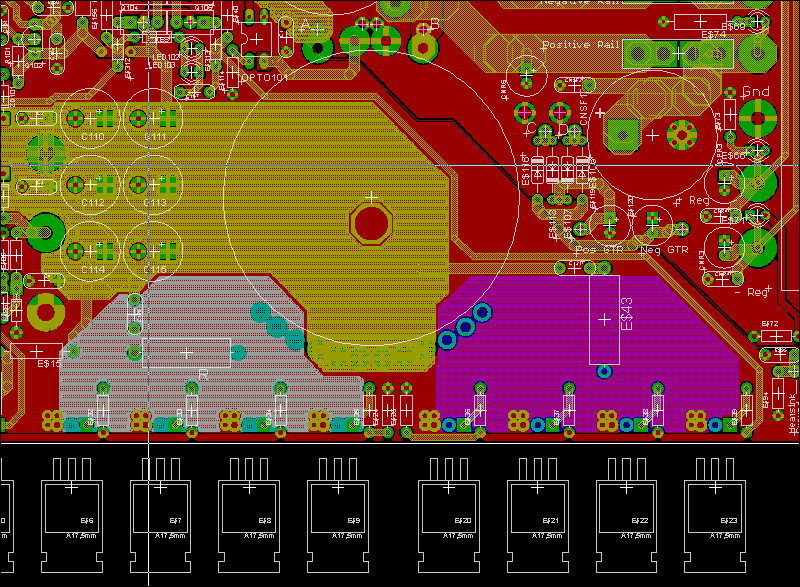
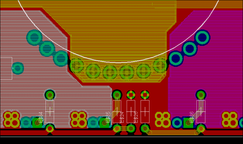
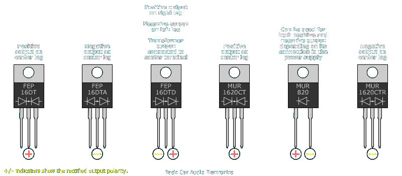
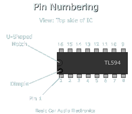
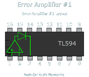
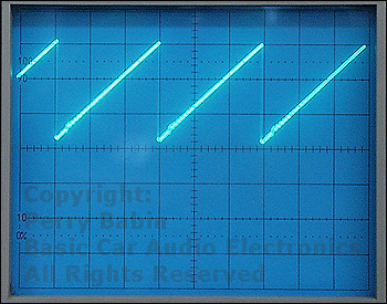
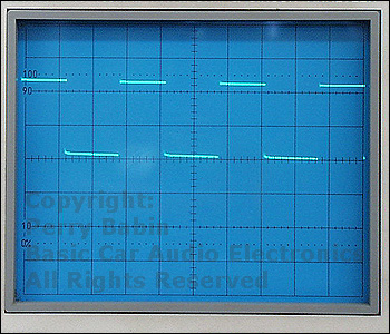
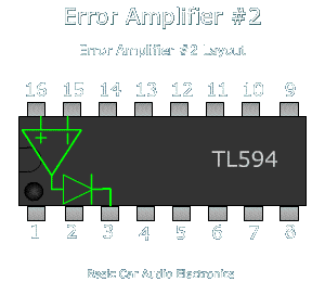
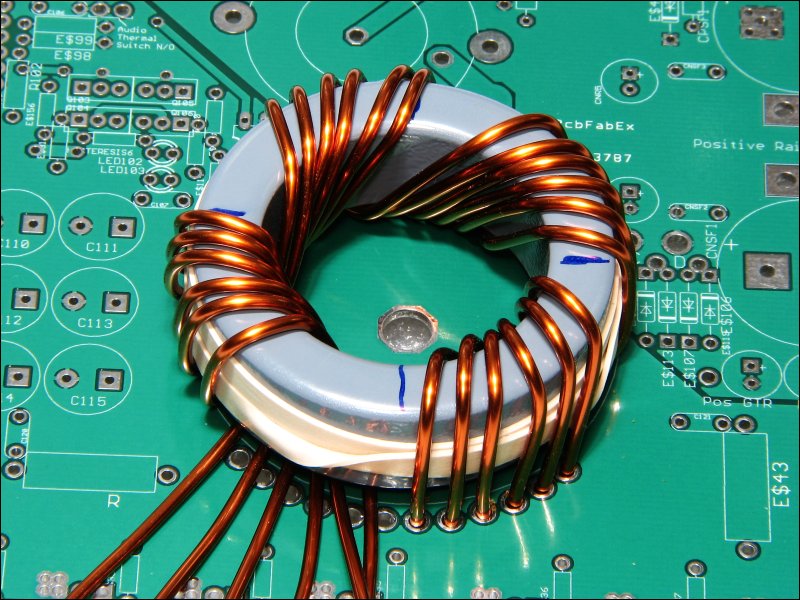
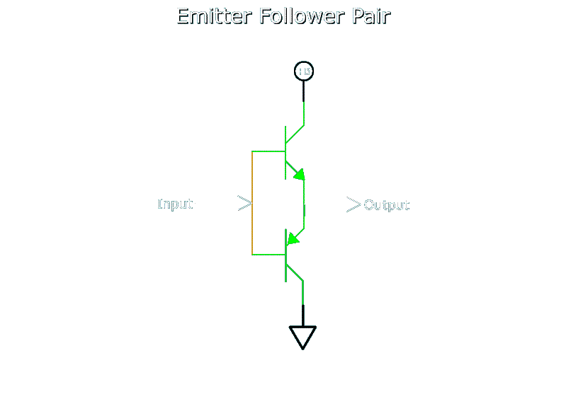
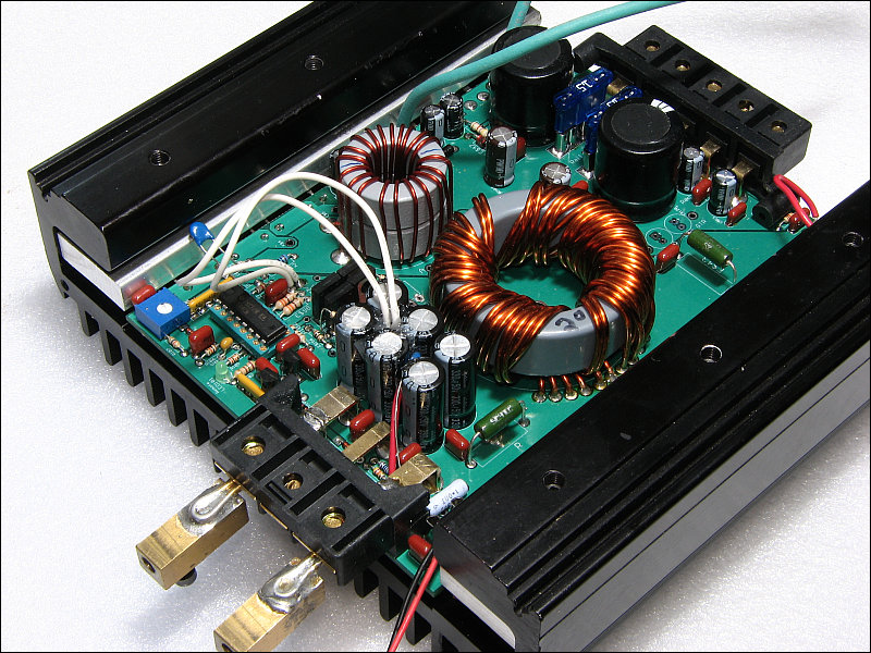

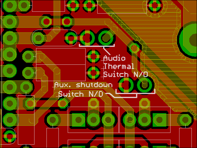
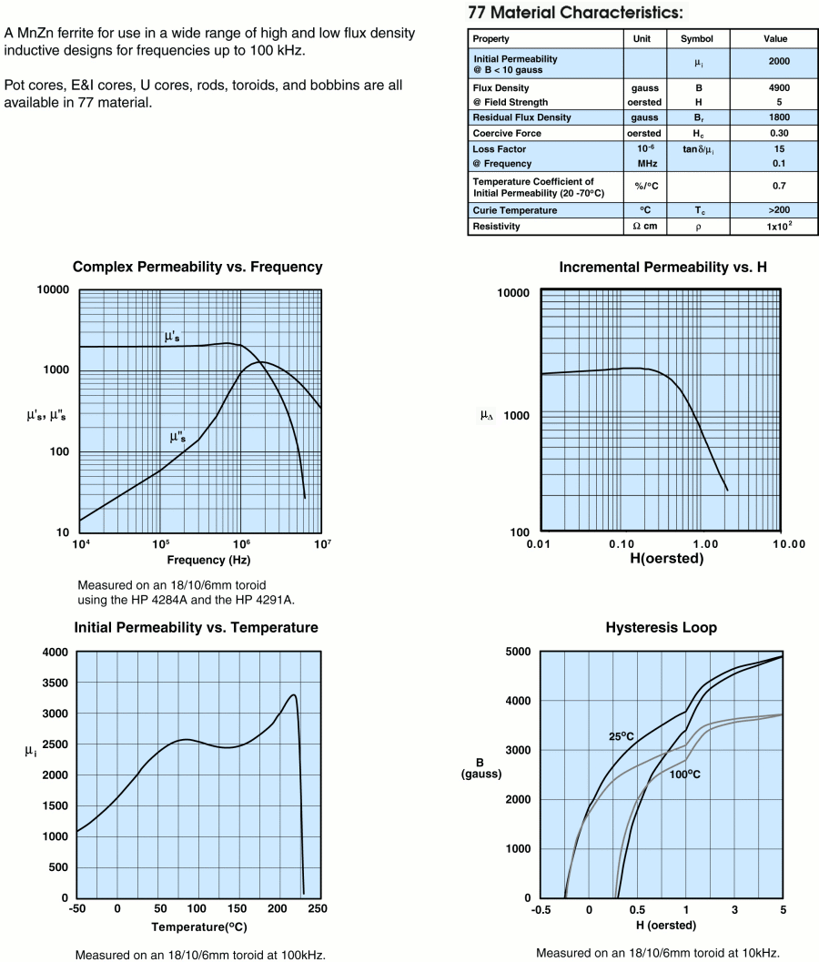